SBAU356 September 2020 ADC3660
2.1 Evaluation Board Feature Identification Summary
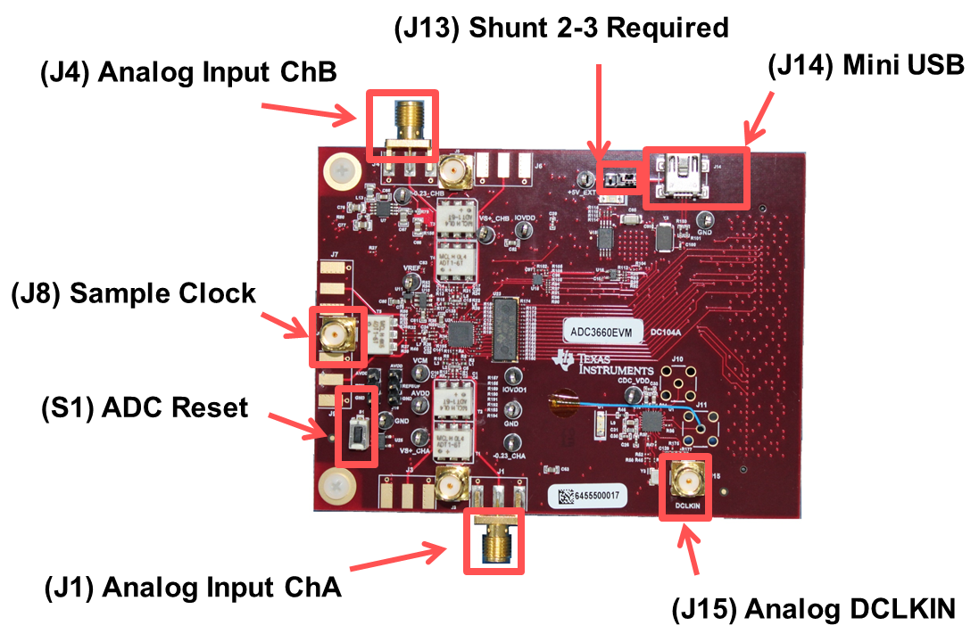
 Figure 2-1 ADC3660EVM Feature Identification.
 Ensure that jumper J8 is shunted in the 2-3 position. This allows 5 V to be supplied to the ADC3660EVM through the mini-USB connector.
If an external 5-V supply is desired, J8 must be shunted in the 1-2 position, and the external 5 V can be connected to the test point labeled "+5 EXT".
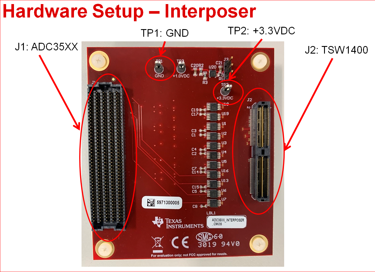
 Figure 2-2 CMOS FPGA Interposer Card.