SBAU361 December 2020 ADC3664
5 Onboard FDA Configuration
By default, the analog input is configured to use the balun input (AD1T-6T+) for both analog input channels, but can be modified to utilize the onboard FDA (THS4541).
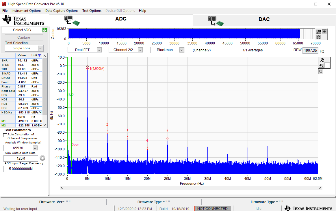
In terms of performance as compared with the balun input, SNR and SFDR are similar up to ~ 15 MHz input frequency. If using input frequencies above 15 MHz, it is recommended to use the balun input.
A benefit of using the FDA is that the required signal strength needs to achieve the full scale input is several dB less when compared to the balun input (losses in 50 ohm termination for balun input).
 Figure 5-1 ADC3664EVM: FDA Input
This procedure shows how to configure the FDA single-ended to differential conversion for CHA. The same procedure can be performed for CHB (with the respective component designators).
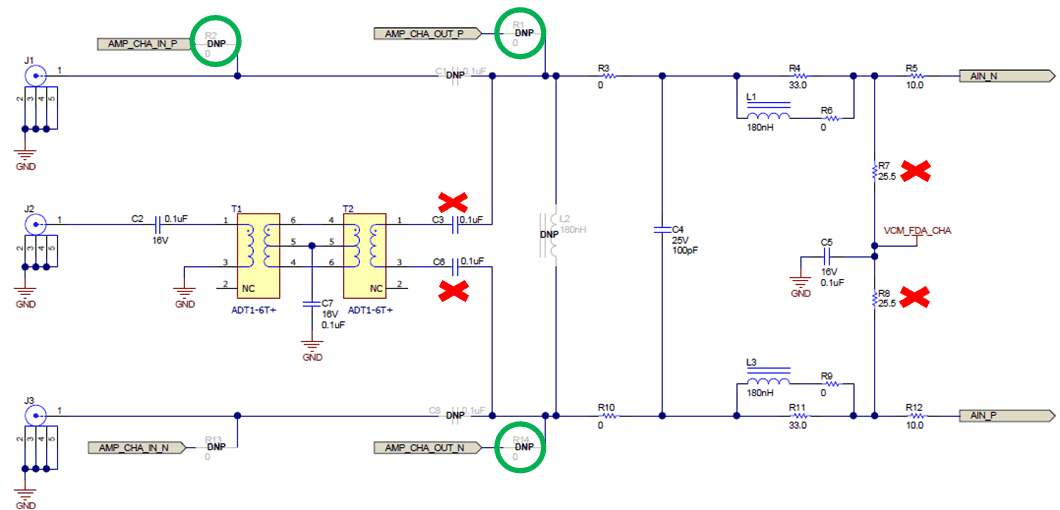
The edge launched SMA connector J1 receives the single-ended analog input signal. R1 can be replaced with a capacitor for AC coupling to FDA.
Modify the following components to complete the path to FDA (located on top of EVM).
- Install: R1, R2, R14 (o Ω)
- Remove (DNI): C3, C6, R7, R8
 Figure 5-2 CHA FDA Component
Modification
Figure 5-2 CHA FDA Component
ModificationThe FDA is setup with a gain of 2.5, and can be adjusted (R78, R84, R86 and R94) as the application requires. There is a 20 MHz LPF on the output of the FDA, and these components (C52, L11,L12 and C53) can be adjusted as the application requires. The termination resistors (R80, R81, R89 and R90) can be adjusted according to the source impedance.
 Figure 5-3 FDA Schematic
For further information on the THS4541 FDA, see the THS4541 Negative Rail Input, Rail-to-Rail Output, Precision, 850-MHz Fully Differential Amplifier data sheet.