SBAU361 December 2020 ADC3664
4.3.1 ADC35XX GUI: Complex Decimation Configuration
Table 4-3 14-Bit, Complex Decimation, Sample
Rate and DCLKIN Examples
| Interface Mode | DCLKIN Multiplier (Serialization Factor) | Example Sample Clock | Complex Decimation Factor | Required DCLKIN Frequency |
|---|---|---|---|---|
| 2 Wire | 3.5 | 125 MSPS | 2 | 437.5 MHz |
| 1 Wire | 7 | 65 MSPS | 8 | 113.75 MHz |
| 1/2 Wire | 14 | 35 MSPS | 32 | 30.625 MHz |
For this 32x Complex Decimation example, apply a 125 MHz signal to J9 (sample clock) and a 27.34375 MHZ signal to J7 (DCLKIN).
Attention: External ADC sampling
clock source and DCLKIN source must be frequency locked. If this is not performed, the
captured data will appear scrambled. If using the onboard clocking option, the sampling
clock and DCLKIN are frequency locked.
Apply a 5 MHz signal to J2 (ensure bandpass filter is used to reduce harmonics and noise of signal generator). An NCO of 4.9 MHz will be used to shift the 5 MHz input signal to -100 kHz.
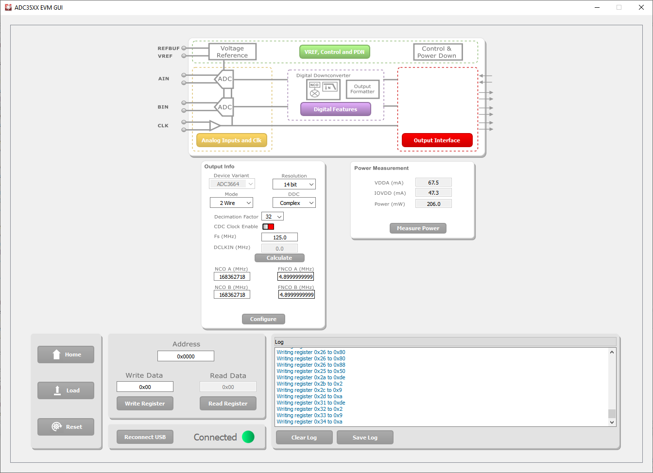
After launching the ADC35xxEVM GUI perform the following steps:
- Under "Resolution", select "14 bit".
- Under "DDC", Select "Complex".
- For "Decimation Factor", select "32".
- Ensure that CDC is disabled (red).
- For "Fs (MHz)", select 125M.
- To calculate the DCLKIN frequency, enter "125" in the Fs (MHz) field, and click calculate. This is informational only.
- Under "FNCO A (MHz)" and "FNCO B (MHz)", enter "4.9" in the field. This field will then calculate to the nearest valid NCO value, and will auto-calculate the correct register values in the field next to it.
- Click "Configure".
 Figure 4-9 ADC35XXEVM GUI: ADC3664EVM
32x Complex Decimation