SBAU396 May 2022
2 ADC-PHI-PRU-EVM Overview
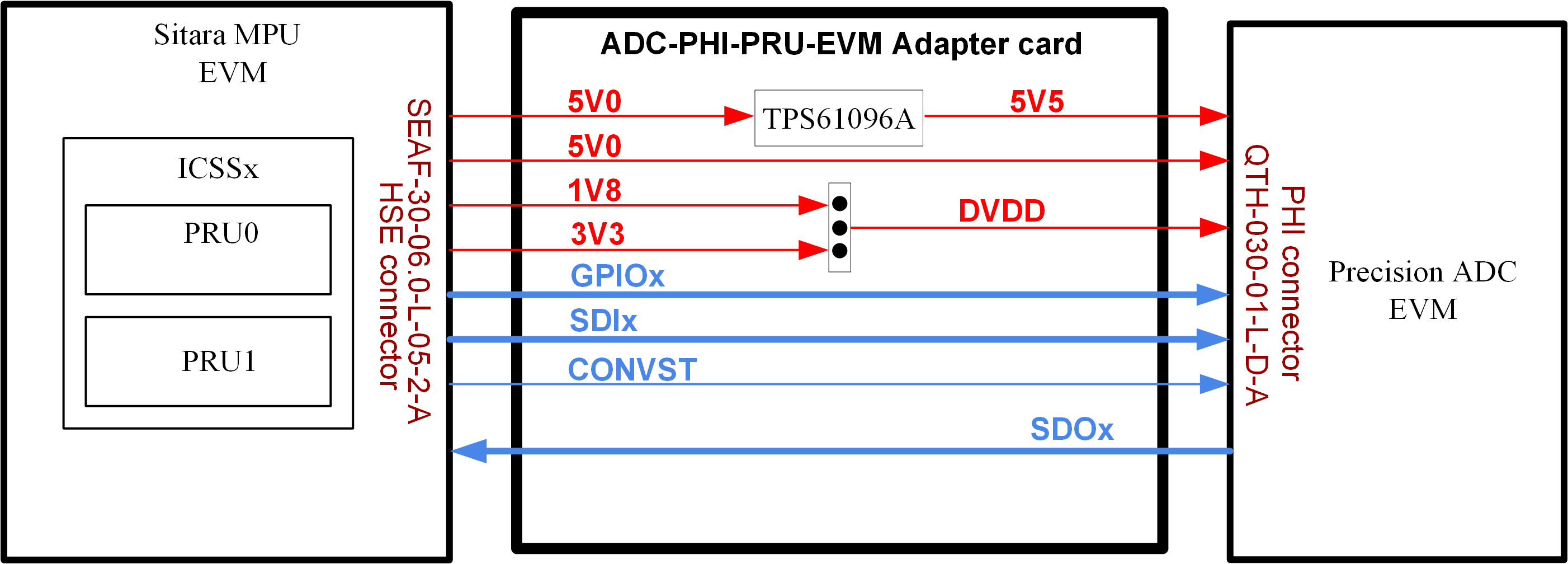
Figure 2-1 shows the two main connectors of the ADC-PHI-PRU-EVM adapter card. The 150-pin high-speed expansion (HSE) connector is on the left and mates with the AM64x and AM243x general purpose (GP) development platform HSE connectors. The 60-pin Q-strip (QSH) connector is on the right and mates with the precision ADC EVMs listed in Table 3-1. Three jumpers (J2, J9, and J11) on the ADC-PHI-PRU-EVM select the following settings:
- J2 shorts the CONVSTA and CONVSTB signals together for operation with a single CONVST signal
- J9 configures the MUX to select either serial or parallel mode to communicate with the precision ADC EVM
- J11 selects either 1.8 V or 3.3 V as the DVDD voltage for the precision ADC EVM
 Figure 2-1 ADC-PHI-PRU-EVM System Architecture