SBOA097B June 2004 – May 2015 INA132 , INA146 , INA152 , OPA2205 , OPA2277 , OPA277 , OPA301 , OPA335 , OPA364 , OPA4205 , OPA725 , TLV2341
2 Circuit 1: The Modular Approach
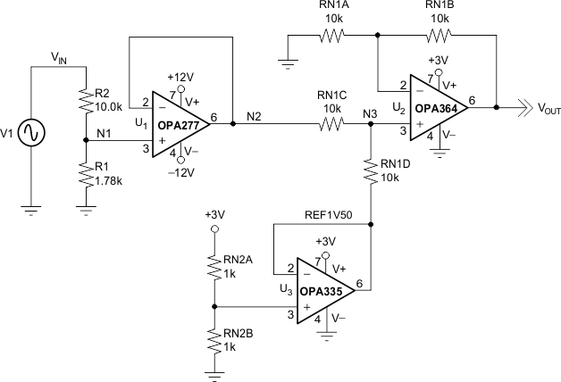
The circuit shown in Figure 1 is a classic modular approach to circuit design. The first stage is attenuation. The second stage is level-shifting. This style is convenient because designers can compartmentalize adjustments. Input range can be adjusted by changing R1. Level-shift can be changed by adjusting REF1V50. These parameters are independent and can be tuned with minimal interactions. Furthermore, designers may want to include anti-alias filtering or other analog functions. These blocks can be neatly inserted at node N2.
 Figure 1. Circuit 1: Modular Design
 On the front-end voltage divider, the equation for R1 is:

In Circuit 1, the following values are used:
- VOUT = 3V
- VIN = 20(±10)V = V1
- R1 = 1.76k (1.78k is closest standard value)
- R2 = 10k
- REF1V50 = midpoint of ADC full-scale input range.
These component values can be altered to account for different input ranges or input impedance requirements. In this example, the value of R2 is held constant to simplify calculations and reduce trimming to one element.
The first stage op amp is an OPA277. The OPA277 was chosen for its low VIO, low drift, and bipolar swing. This stage needs to have bipolar swing about ground because the input signal is bipolar. The OPA277 is also a great candidate for active-filter stages. TI's free FilterPro design tool (available for download at www.ti.com) can be used to design and model active filters. FilterPro presumes that the amplifiers under consideration are operating in a bipolar mode, making node N1 the appropriate place for filters. Another option for the first stage is the OPA725, which is suitable for bipolar stages with ±5V rails.
The second stage op amp is the OPA364. This outstanding, low-voltage op amp offers many assets which are ideal at this stage: it is low-voltage and low-power, in addition to having a large input common-mode voltage range. It also has zero crossover distortion for linear, monotonic, large-signal output.
Resistor networks are used to bias the OPA364 and the reference because they are matched. This ratiometric design takes advantage of this property. Gain errors from mismatched components cannot be distinguished from genuine signals. For example, the gain error from discrete 1% components is equivalent to –40dB of erroneous signal. This is inadequate for 12-bit, or higher, conversions, where the minimum detectable signal is below –70dB. Resistor networks with ratio 0.01% tolerances (–80dB) are readily available. High-quality metal foil networks with 0.005% tolerances (–106dB) may be necessary for extreme cases.
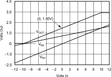
The DC sweep plot of Circuit 1 is shown in Figure 2. Node N3 shows the input common-mode voltage swing of the second stage.
 Figure 2. DC Sweep of Circuit 1
 Designers may want to consider the INA132 or the INA152 for the second stage. These amps are considerably slower than the OPA364, but they come with precision-matched internal resistors to reduce gain errors. In general, DC precision is desirable for open-loop applications such as temperature sensors or calibrated transducers, where absolute accuracy, offset and drift are critical. This precision makes the INA132 a good choice for absolute measurements. In closed-loop applications such as servos loops or PID controllers, high-speed and monotonicity are desirable. In closed-loop systems, DC offsets and gain errors will be canceled by feedback and calibration. This makes the OPA364, or the OPA301, a good choice for servos and feedback signals.