SBOA443 March 2021 INA293
2.1 Acquisition Time
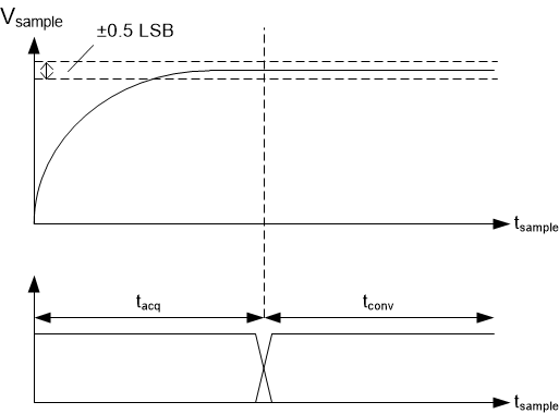
When examining the sampling scheme for a SAR ADC, it is broken down into two specific time frames: acquisition time, and conversion time. The relative flow of the capture of a single sample is shown in Typical ADC Single Acquisition Cycle , and the input structure of the ADS8860 is shown in ADS8860 Input Sampling Stage Equivalent Circuit, Hold Mode below.
 Figure 2-1 Typical ADC Single Acquisition Cycle
 Figure 2-2 ADS8860 Input Sampling Stage Equivalent Circuit, Hold Mode
At the beginning of the acquisition phase, the switches of the sample and hold input structure close allowing the sample and hold capacitor, CSH, to charge. This capacitor will continue to charge until it either settles to a final value, or the end of the acquisition period is reached, at which point the switch re-opens and conversion begins. The goal of a successful design is to ensure that this sample is sufficiently charged within the acquisition window of the ADC, to prevent any additional error greater than the quantization noise of the ADC on the measurement.
Immediately following the acquisition time, the ADC begins operation on the sampled value and digitizes the information. The time in which this occurs is called the conversion time. This is the time required by the ADC to convert the measured result into a digital value. Once this value is completed, it is delivered to the host processor, and the next sample and hold cycle begins.
The conversion time for any ADC is typically a fixed value inherent to the device, and remains fixed regardless of the value of the sampling clock.