SBOA510 March 2021 OPA455 , OPA462
- Trademarks
- 1Introduction
- 2Three Op Amp OPA462 HV Solution
- 3Lower Voltage, Lower Cost Three Op Amp Solution
- 4OPA462 300 Vpp Output Solution With Discrete Transistor Supply-Rail Drivers
- 5Lessons Learned from the Practical Implementation of the HV Op Amp Solutions
-
A Appendix
- A.1 Overview
- A.2 Summary of Results
- A.3 Test Setup and Equipment
- A.4 Printed Circuit Boards
- A.5 Power Supply, Source Measurement Unit (SMU)
- A.6 Arbitrary Waveform Generator (AWG)
- A.7 Oscilloscope
- A.8 Circuit 1: OPA462 Three op amp Solution
- A.9 Circuit 2: Lower Voltage, Lower Cost Three Op Amp Solution
- A.10 Circuit 3: OPA462 300 Vpp Output Solution With Discrete Transistor Supply-Rail Drivers
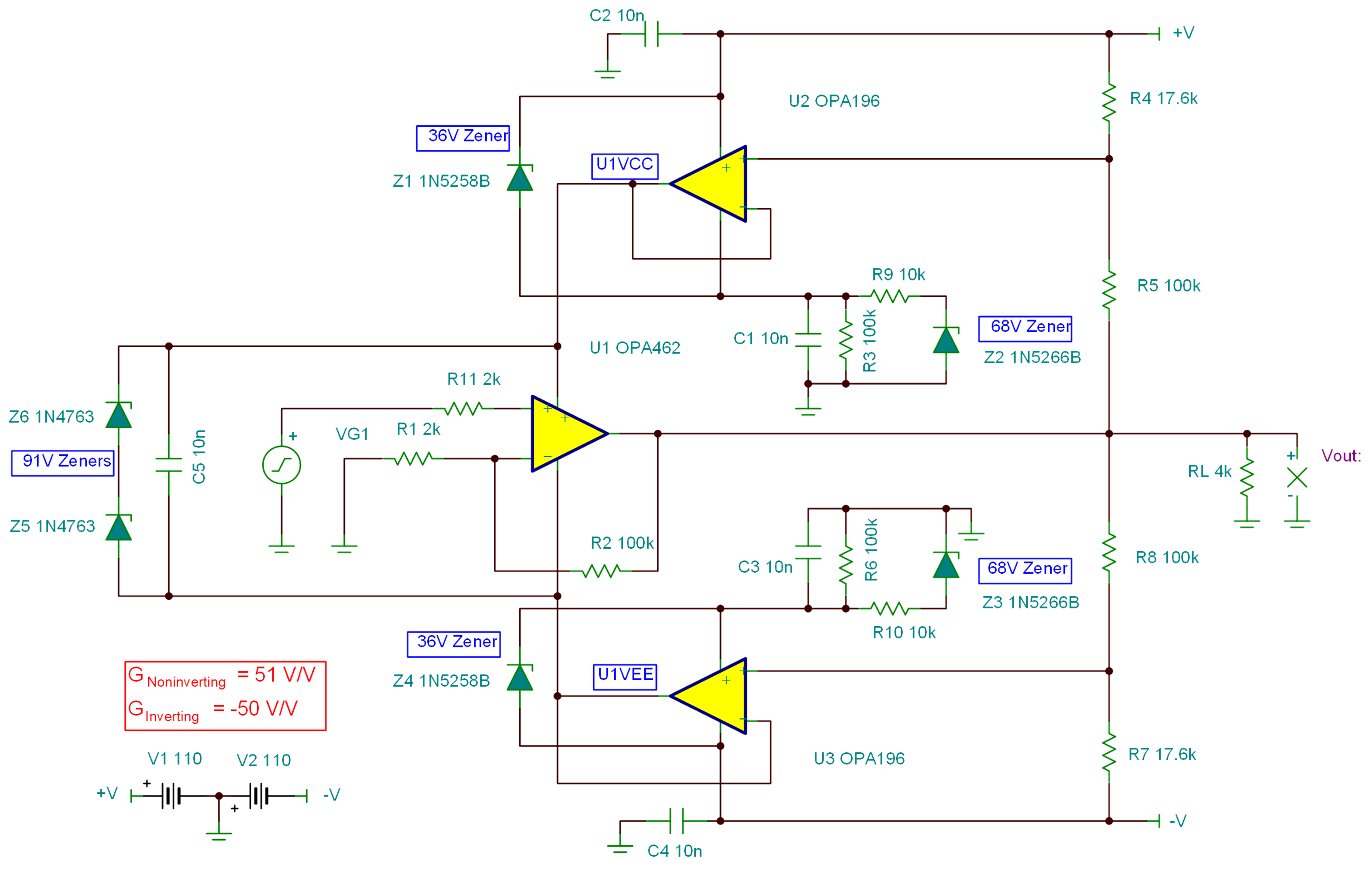
A.9.1 Schematic
 Figure 6-8 Lower Voltage, Lower Cost Three
Op-amp Solution