SBOA521 June 2021 OPA3S328
4 Stability of the Transimpedance Amplifier
The circuit designer must verify the minimum necessary op-amp gain-bandwidth to guarantee stability and select the appropriate feedback compensation capacitor for each TIA gain. Therefore, it is essential to consider factors that affect TIA circuit stability carefully: the junction capacitance of the photodiode (CJ), the TIA gain, the desired closed-loop TIA bandwidth, and the unity gain-bandwidth product of the op-amp (fGBW).
The circuit diagram on Figure 4-1 shows the photodiode reverse junction capacitance (CJ) and the differential and common mode input capacitance of the of-amp (CDIFF, CCM1,2).
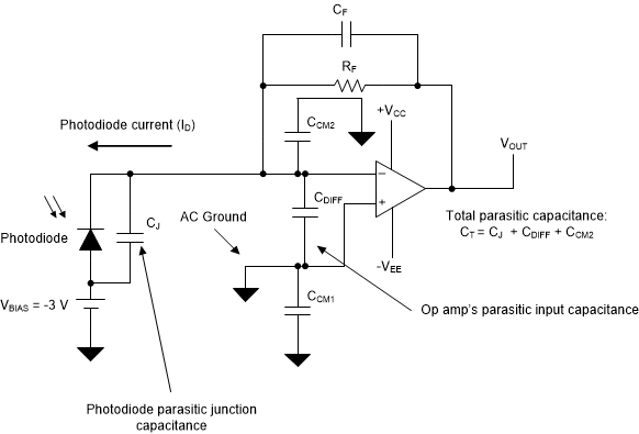 Figure 4-1 Photodiode Transimpedance Amplifier and Total Parasitic Capacitance
Figure 4-1 shows the total capacitance at the input of the amplifier. This capacitance is the parallel combination of the photodiode capacitance, and the amplifier differential and common-mode input capacitance. Since the non-inverting terminal connects to an AC ground, the CCM1 common-mode capacitor does not contribute to the total input capacitance:

The OPA3S328 offers a differential capacitance of approximately, CDIFF = 3.8pF, and the common-mode capacitance, CCM2 = 1.2pF. Accounting for the photodiode junction capacitance, the total capacitance at the input of the amplifier CT is approximately 105pF.
The TIA circuit stability is related to the amplifier’s loop gain and the loop gain phase response. The loop-gain is the product of the op amp’s open-loop gain (AOL) and the circuit feedback factor (β), where the circuit’s loop-gain is (AOL * β). Phase margin is a stability metric which compares the phase of the loop-gain (AOL * β) of an amplifier to 180 degrees at the point where loop gain equals 0-dB and marks the frequency where AOL and the 1/ β bode plots intersect.
One method to determine the stability of the circuit is called the rate of closure analysis. In this method, we consider the rate of closure of AOL and 1/ β at frequency fC, the point in frequency where the magnitude plots intersect. This method's rule is that the difference in the slope of the AOL magnitude and the slope of the 1/ β magnitude plots must be ideally close to 20-dB or less to ensure optimal stability.
Figure 4-2 shows the bode plots of the AOL for a high bandwidth amplifier and the AOL for a lower bandwidth amplifier, along with the 1/β curve of a typical TIA.
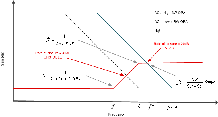 Figure 4-2 AOL and 1/β plot for Transimpedance Op Amp Circuit
The 1/β magnitude plot, also referred to as the non-inverting gain or noise gain, presents a zero (fZ) and a pole (fP) on its frequency response. Above the zero frequency (fZ), the 1/β plot increases a rate of +20dB per decade. At frequencies above the pole (fP), the 1/β curve remains flat. The frequency fC is the frequency point where the AOL and 1/β magnitude plots intersect, and this frequency is a function of the unity gain-bandwidth product of the amplifier fGBW, the feedback capacitor, CF, and the total input capacitance of the amplifier, CT:

By analyzing the rate of closure (ROC) of AOL and 1/β when the curves intersect, we can determine the stability of the circuit. The rule of thumb for this method is that the rate of closure must ideally be close to 20-dB/decade for optimal stability. Therefore, to maintain stability, the AOL curve must intersect the 1/β curve when the 1/β curve is flat. If the AOL curve intersects the 1/β curve when the 1/β curve is rising, as shown by the lower bandwidth op amp AOL curve in Figure 4-2, the rate of closure is 40-dB and the circuit will likely be unstable, leading to unwanted oscillations, long settling time and intermittent or unfavorable circuit behaviors.
Equation 5 provides the necessary condition for the transimpedance amplifier stability:

Substituting the equations for fC and fP into the inequality provided on Equation 5 yields to Equation 6

The inequality can be re-arranged as a quadratic equation in terms of the feedback capacitor, CF, as shown in Equation 12:

Solving for CF using the general quadratic formula and obtaining the only real positive solution yields the result shown in Equation 8:

Equation 8 determines the minimum compensation capacitor to guarantee stability for the TIA design. Table 4-1 shows the minimum calculated compensation capacitors CF1 and CF2 to ensure stability for each TIA gain for the unity gain-bandwidth of the OPA3S328. The dominant pole frequency fP is a function of the feedback resistor and feedback capacitor for each TIA gain.
| fGBW Amplifier Unity Gain Bandwidth |
TIA Gain | CT TIA Total Input Capacitance |
RF TIA Feedback Resistor |
CF Min Feedback Capacitor for stability |
fP Dominant Pole frequency |
|---|---|---|---|---|---|
| 40 MHz | 200 kV/A | 105 pF | 200 kΩ | >1.5pF | 530kHz |
| 40 MHz | 2 kV/A | 105 pF | 2 kΩ | >16pF | 4.97MHz |
A different approach to ensure stability while meeting a TIA gain and bandwidth requirement, is to use the inequality provided in Equation 6, and solve for the amplifier's minimum unity gain-bandwidth (fGBW). Equation 9 provides the amplifier's minimum fGBW as a function of the feedback resistor RF, the feedback capacitor CF, and the total input capacitance of the amplifier CT:

Equation 9 determines the amplifier's minimum required unity gain-bandwidth to guarantee stability for a TIA design. Therefore, higher bandwidth amplifiers support higher gain and bandwidth TIA circuits, and tolerate higher photodiode capacitance while remaining stable.
On this programmable gain TIA example, the desired closed-loop bandwidth TIABW is 500kHz. Therefore, Equation 10 provides the maximum compensation capacitance CF while meeting the closed loop TIA bandwidth requirement:

Equation 10 shows the calculated compensation capacitors CF1 and CF2 for each gain to meet the TIA closed-loop bandwidth requirement and the required amplifier's minimum unity gain-bandwidth to ensure stability:
| TIA Gain | TIABW Desired TIA Bandwidth |
CT TIA Total Input Capacitance |
RF TIA Feedback Resistor |
CF Feedback Capacitor for TIABW |
fGBW Min Amplifier Unity Gain BW |
|---|---|---|---|---|---|
|
200 kV/A |
500 kHz |
105 pF |
200 kΩ |
1.6pF |
> 33.8MHz |
|
2 kV/A |
500 kHz |
105 pF |
2 kΩ |
159pF |
> 834 kHz |
The OPA3S328 offers a unity gain bandwidth of 40 MHz, and therefore, can support the desired TIA gain and bandwidth requirements for the design. Select standard values for the compensation capacitor, CF1 = 1.6pF for TIA gain of 200kV/A and CF2 of 150pF for TIA gain of 2kV/A.
Verify the stability for each gain using TINA SPICE simulations. Figure 4-3 shows the TINA-TI circuit schematic used to analyze stability. Use a large inductor (L1) to break the loop at the input of the amplifier. The test voltage source is AC coupled through the large capacitor (C1). Since the feedback loop is open at the op-amp input, add the op-amp input capacitance, CDIFF and CCM2 into the schematic next to inductor L1. Use the simulator post-processor to generate the open-loop gain (AOL) and noise gain (1/β) curves for each gain setting. Figure 4-4 shows the stability analysis simulation results for RF1 = 200kΩ, CF1 = 1.6pF and Figure 4-5 for RF2 = 2kΩ, CF2=150pF.
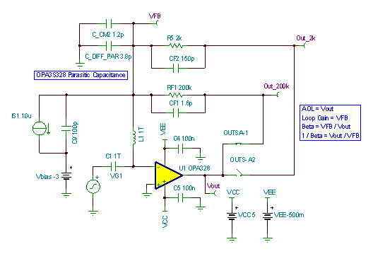 Figure 4-3 TINA-TI Circuit Schematic to Analyze Programmable Gain TIA Stability
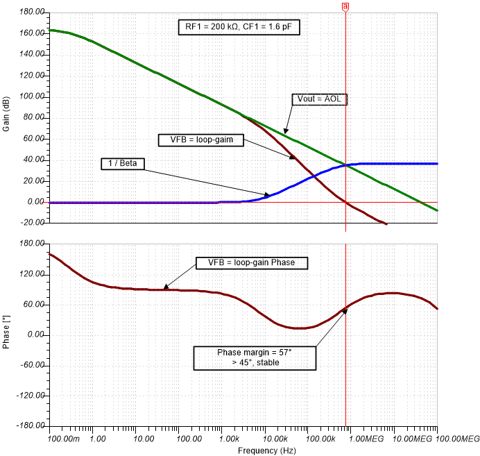 Figure 4-4 Stability Analysis for RF1 = 200kΩ
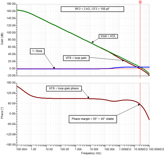 Figure 4-5 Stability Analysis for RF2 = 2kΩ