SBOA521 June 2021 OPA3S328
5.2 TIA Output Swing and Switch On-Resistance
When building a programmable gain TIA with analog switches, the circuit designer needs to account for the voltage drop across the switch RON resistance when the photodiode current flows through the amplifier's feedback. This voltage drop is significant at the higher photodiode current ranges.
Amplifier output stages that can swing close to the complete span between negative and positive supply voltage are generally known as rail-to-rail output (RRO) stages. Most RRO stages can swing within tens of millivolts of the rails. The amplifier's data sheet specifies the output voltage range from the supplies as output swing (output voltage low/high). Although the OPA3s328 offers an RRO stage and the amplifier functions in this region, the performance gradually degrades as the output gets closer to the rails where the amplifier open-loop gain decreases. Therefore, it is advisable to allow extra headroom in applications that require very low distortion. A conservative approach to ensure the amplifier remains well within its linear region is to use the output swing headroom from supply from the data sheet open-loop gain (AOL) specification:
| Parameter | Test Condition | Min | TYP | Max | Unit |
|---|---|---|---|---|---|
| AOL Open-loop voltage gain |
(V–) + 200 mV < VO
< (V+) – 200 mV RL = 2 kΩ |
108 | 123 | dB |
The OPA3S328 data sheet output swing specification during the AOL test is 200mV from the rail with a 2kΩ load referred to mid-supply, while the device is powered with a 5.5V supply. This AOL test condition corresponds to an equivalent load current of approximately 1.275mA. In this TIA example, the OPA3S328 sources a maximum of 2mA of current, therefore, the designer must allow headroom exceeding >200mV.
The designer must carefully choose the maximum feedback resistor to meet the minimum headroom requirement. Equation 12 provides the maximum TIA feedback resistor value (RF) as a function of the supply voltage (VCC), the maximum diode current (ID_Max), the maximum on-resistance (RON_Max) while allowing the necessary output swing supply headroom (VHeadroom).

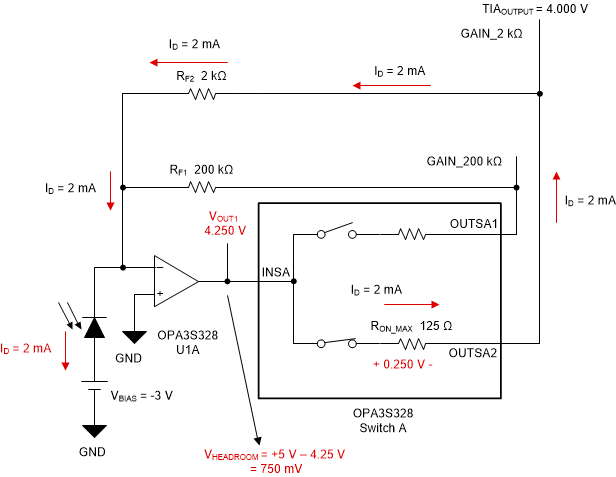
In this example, the calculation yields a resistance less than <2275Ω for a max current of 2mA, max on-resistance of 125Ω, allowing a 200mV headroom from the supply. For the circuit design, we choose RF2 =2kΩ exceeding the minimum headroom condition. Figure 5-6 shows the voltage drop across the worst-case RON_Max resistance of 125Ω with ID_Max = 2mA and the resulting output swing headroom.
 Figure 5-6 Switch RON
Resistance and Output Swing Headroom