SBOA523 July 2021 TMP390 , TMP392
1.1 Temperature Switch Design Using Discrete Components
There are many important factors to consider when designing a temperature switch, for example; size, cost, the range of operation (minimum and maximum temperatures), ease of use (threshold adjustments), and so forth. Figure 1-2 shows an example of a temperature switch design.
This design uses the TLV9002 dual-channel op amp (a comparator would work as well) and two negative temperature coefficient (NTC) thermistors. All other resistors either bias the circuit and set the reference points for the desired operation or create hysteresis. RT1 and R3 create a voltage divider that is fed into one of the inverting inputs of the op amp while R1 and R2 create a voltage divider that is fed into one of the noninverting inputs of the op amp, such that when the voltage generated between RT1 and R3 is greater than the voltage generated by R1 and R2, the output TRIPA_1 goes low. Inversely, when the voltage generated between RT1 and R3 is less than the voltage generated by R1 and R2, the output TRIPA_1 goes high. Since the output logic is active low and RT1 is an NTC thermistor, this would imply that the output TRIPA_1 represents a hot temperature threshold. Using the same logic with RT2 and R7 and R5 and R6, one can reasonably conclude that TRIPB_1 represents a cold temperature threshold. R4 and R8 function to create hysteresis for the hot and cold thresholds, respectively. The values of the components have been calculated to result in a hot threshold of 80°C with 10°C of hysteresis and a cold threshold of –40°C with 10°C of hysteresis.
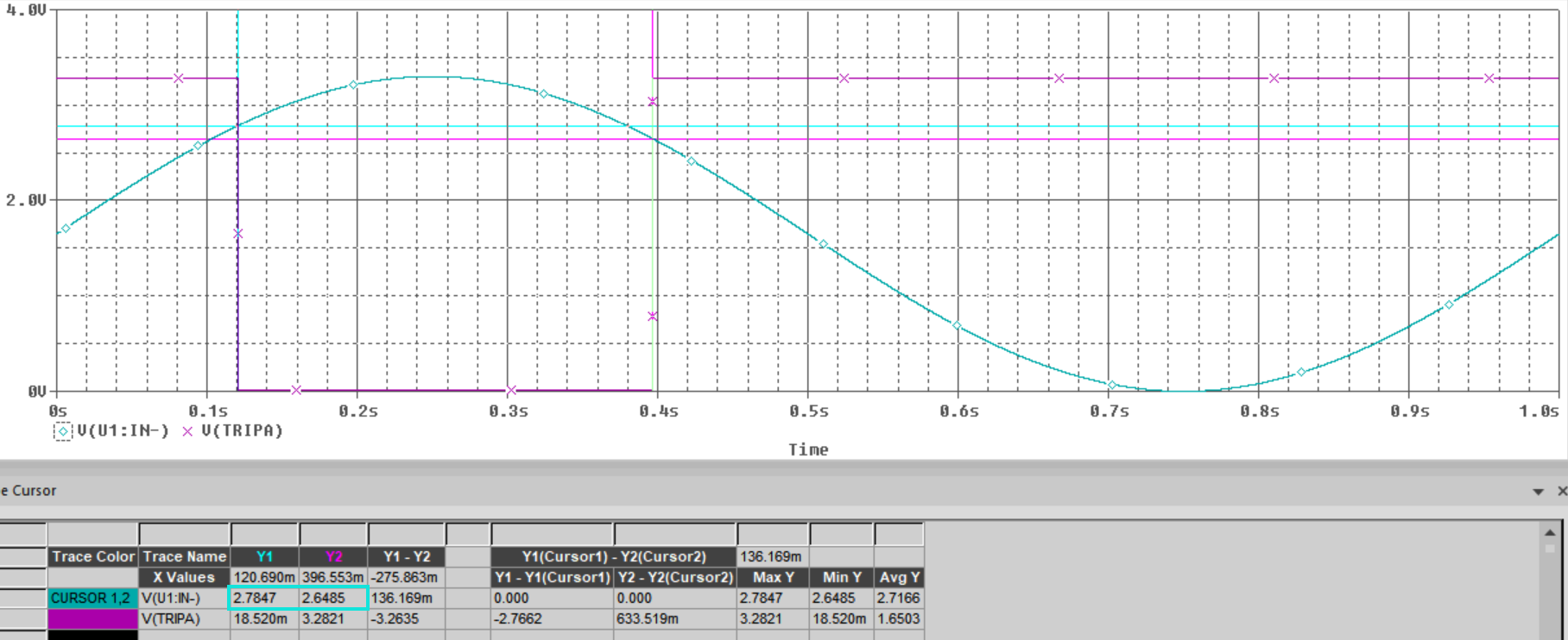
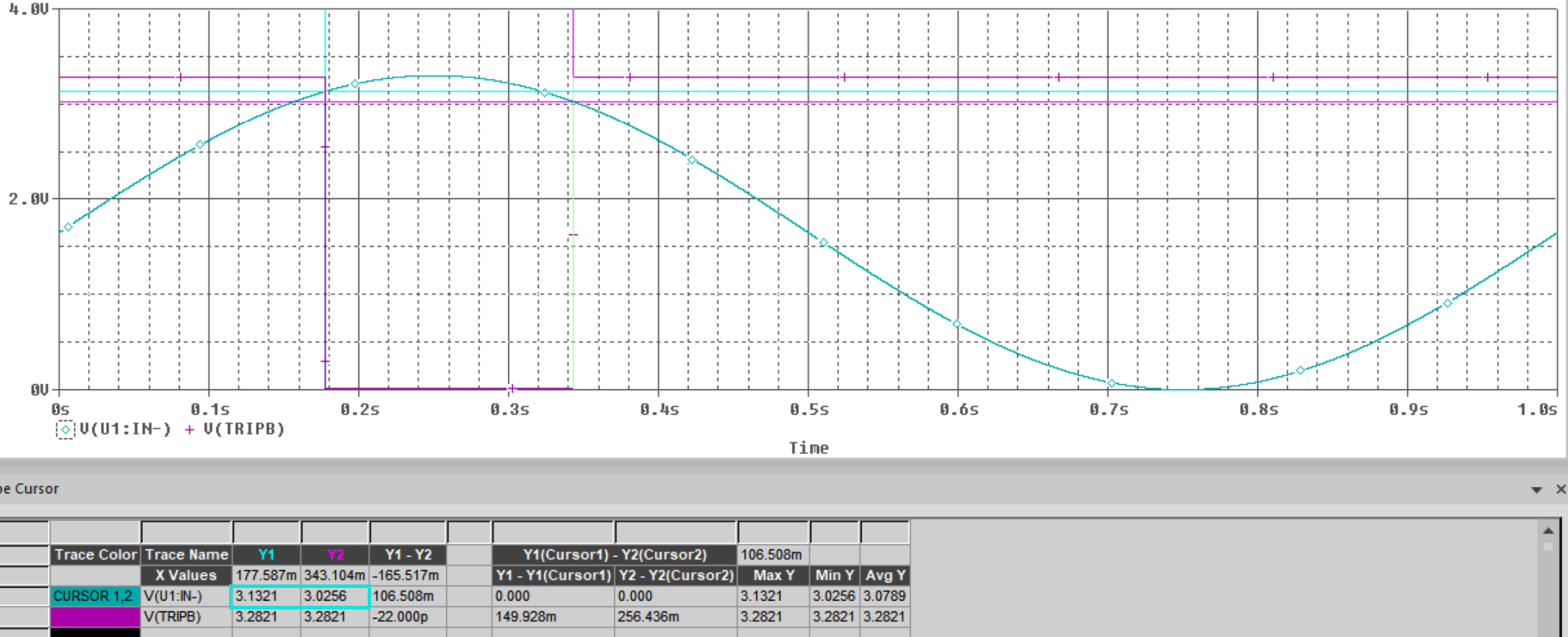
A PSPICE simulation of the circuit in Figure 1-2 results in the waveforms seen in Figure 1-3 and Figure 1-4 of the TRIPA_1 output and the TRIPB_1 output, respectively. It should be noted that instead of the voltage dividers created by RT1 and R3 and RT2 and R7, a sinusoidal input was applied to mimic the behavior of the voltage divider, so the functionality of the circuit remains the same.
 Figure 1-3 PSPICE Simulation Result of
TRIPA_1 Output
 Figure 1-4 PSPICE Simulation Result of
TRIPB_1 Output
Figure 1-4 PSPICE Simulation Result of
TRIPB_1 OutputThese waveforms are consistent to the desired behavior discussed about Figure 1-1. Furthermore, it can be observed that when the sinusoidal input reaches a certain voltage, the output goes low, then goes high again when the sinusoidal input voltage reaches another certain voltage. For example, in Figure 1-3, these voltages are 2.7847 V and 2.6485 V, highlighted by the light blue box. These values can be understood by analyzing the voltage divider created by RT1 and R3; at 80°C, the NTC thermistor has a resistance of 1.669 kΩ. Therefore, the inverting input of the op amp detects a voltage of 2.828 V. Since 80°C is the hot threshold, the output should go low at 2.828 V, in which it does at a voltage of 2.7847 V (the discrepancy between these two values can be attributed to non-ideal resistors and using standard resistor values). There is also a desired hysteresis of 10°C, so the output should go high at 70°C. At 70°C, the NTC thermistor has a resistance of 2.228 kΩ. Therefore, the inverting input of the op amp detects a voltage of 2.699 V, and the output should go high at an input voltage of 2.699 V, in which it does at a voltage of 2.6485 V (again, the discrepancy between these two values can be attributed to non-ideal resistors and using standard resistor values). Therefore, the measured voltages are consistent with the desired operation. In systems that require high accuracy switching, the voltage discrepancies may present an issue. In this case, the voltage discrepancies result in a maximum error in trip point of 4°C.
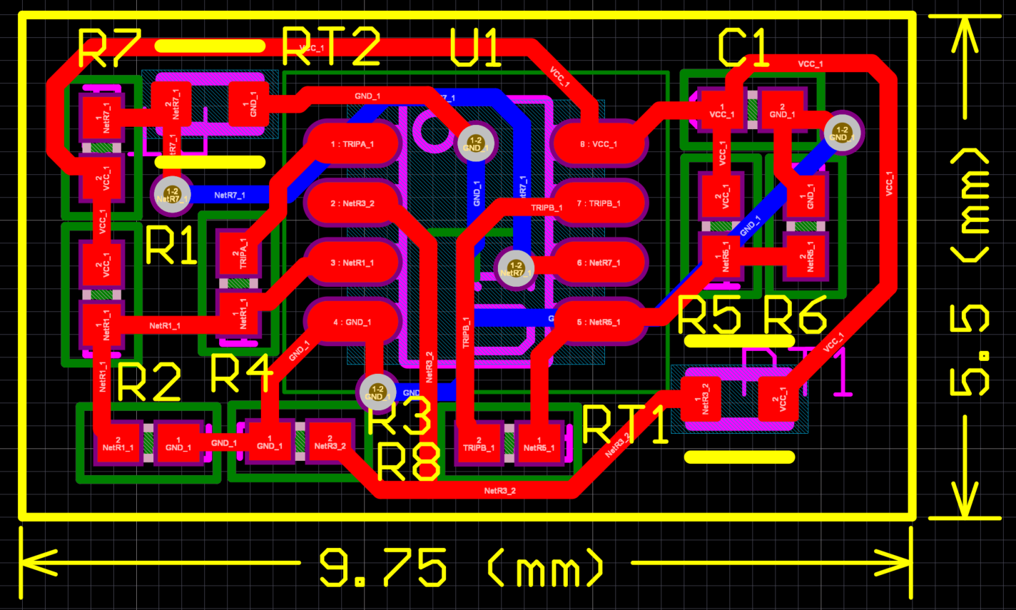
The design presented in Figure 1-2 results in the layout shown in Figure 1-5. Making the layout as compact and consolidated as possible, the minimum area obtained is 53.6 mm2. At temperatures of 25°C, 85°C, and –10°C, this design results in approximate supply quiescent currents of 542 μA, 788 μA, and 337μA, respectively.
 Figure 1-5 Temperature Switch
Layout
Figure 1-5 Temperature Switch
LayoutThe TMP61 is a linear thermistor that operates with a positive temperature coefficient and can offer better accuracy and a smaller design due to its linearity and low tolerance. Figure 1-6 shows the schematic of the temperature switch using the TMP61. This design is very similar to the previously-outlined design while providing the same specifications.
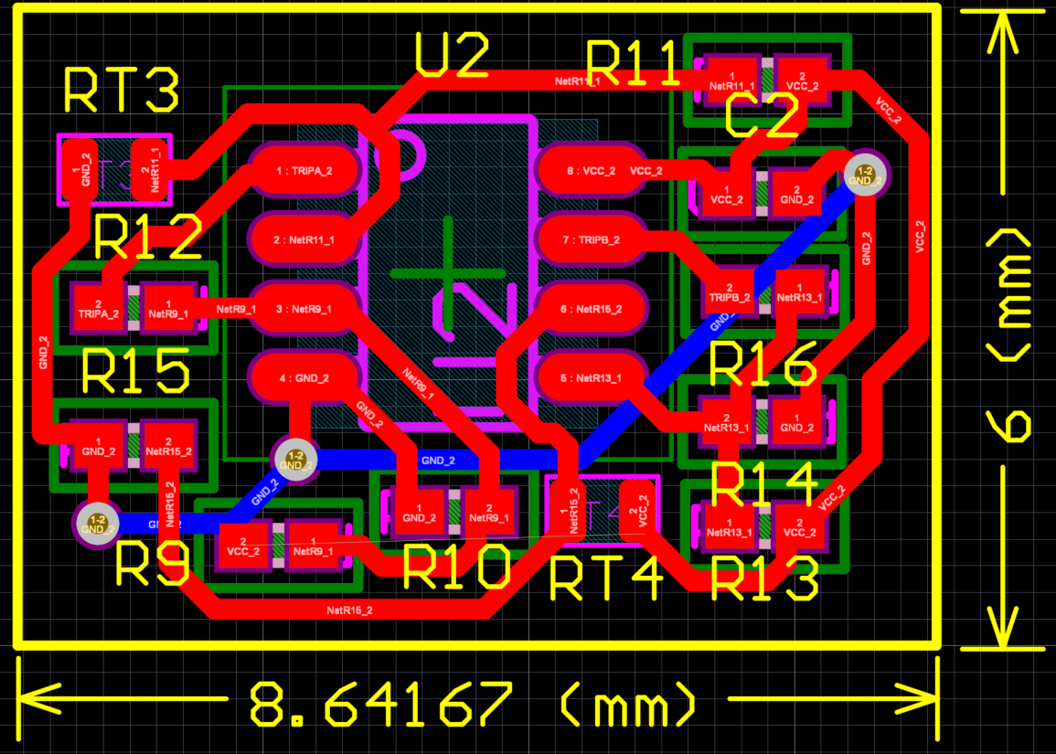
This design results in the layout shown in Figure 1-7. Making the layout as compact and consolidated as possible, the minimum area obtained is 51.9 mm2, which is smaller when compared to using an NTC thermistor. At temperatures of 25°C, 85°C, and –10°C, this design results in approximate supply quiescent currents of 728 μA, 673 μA, and 765 μA, respectively.
 Figure 1-7 Temperature Switch Layout
Using the TMP61