SBOA527 November 2021 INA901-SP
2 Low-Side Implementation
A straightforward design process for the INA901 is presented in the Space-Grade, 50-krad, Low-Side Bidirectional Current Sense Monitor application brief. Use this application note to create the needed reference voltage. When designing with the INA901, ensure that the sense voltage is maintained above 20 mV, because the optimal performance of the INA901 is achieved when operation occurs above this condition.
The design begins with the need to establish an offset point similar to that provided by the REF pins of a bidirectional current amplifier. Under normal unidirectional conditions, resistors on the sense lines are typically discouraged, due to the fact that these resistors can add an offset to the measurement; this results in additional gain error due to discrepancies between the voltage produced on the shunt, and the voltage ultimately observed at the pins of the amplifier. It is possible; however, to use this as a design advantage, and purposefully produce a known offset about which the shunt voltage will swing.
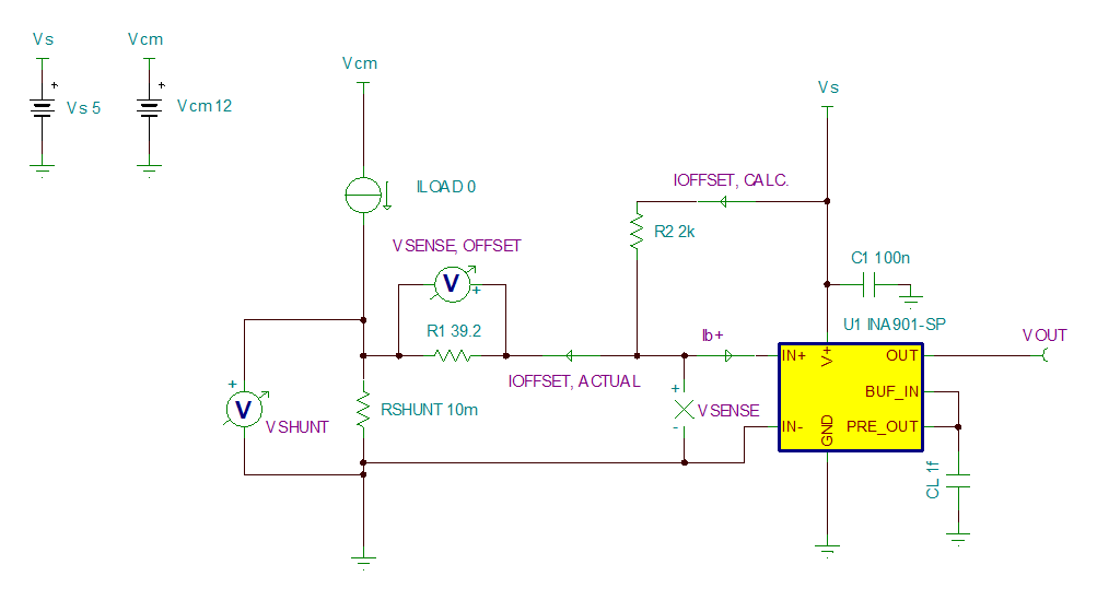
The circuit demonstrates this by creating a precise offset current that flows across an offset resistor, shown as R1 in INA901-SP Low Side Bidirectional Implementation. For the low-side implementation, as the common mode of the inputs is approximately GND, then the needed current can easily be created via a pathway off of supply, using a second resistor, R2, to establish the needed current value. In this topology, it must be noted that the current created is modified by the input bias current, denoted in the schematic as "Ib+", as this is still needed by the INA901 to maintain linear operation. The sense voltage, VSENSE, will also cause IOFFSET to deviate slightly, and therefore slightly shift the offset point over the range of measurement. These changes are small enough; however, that they are still within an acceptable margin of error. Disregarding the bias current, Equation 6 shows that the calculated offset may be approximated as the actual offset current seen by R1.
The value attained relaxes calculation. Begin by choosing desired values for R1 and R2 to establish the desired offset. With the approximation that the effects of the input bias currents are negligible, these resistors provide two potential variables to write linear equations to achieve the desired reference point. This is established in Equation 2 through Equation 4:
The established referred to input (RTI) offset from Equation 2 is presented to the pins of the INA901 as a relatively constant positive voltage which produces an offset, and the voltage created on VSHUNT will either add or subtract from this quantity, based on the direction of current flow. This offset is then acted on by Equation 3, producing the actual output quantity of REF on the output of the INA901.
As an example, consider a system measuring –7.5 A to 7.5 A bidirectionally. Choosing a 10-mΩ shunt, the expected range of VSHUNT produced will ideally be –75 mV to 75 mV. To this range of values, add an appropriate offset voltage, referred to the input. It is important to note that VSHUNT does not equal VSENSE here, as VSENSE (the voltage seen by the sense pins of the INA901 and ultimately gained by the amplifier) will be modified by the created offset voltage.
Utilizing Equation 2 through Equation 4, the values of IOFFSET = 2.5 mA (R2 = 2 kΩ, from the 5-V supply node), and R1 = 39.2 Ω were selected to produce a 1.96-V offset. The initial design conceptualized a 2-V offset from a 40-Ω resistor, but the closest commercially available resistor option is 39.2 Ω. Additional combinations may result in more numerically convenient options if investigated, or custom resistors may be sought at an increased cost of design. From Equation 2, the RTI offset is calculated using Equation 5.
Applying this voltage to the previously-designed input range, the expected design should now produce a VSENSE range of 23 mV to 173 mV, or 460 mV to 3.46 V at the output of the INA901, assuming an ideal gain of 20 V/V. Note that this range was designed to ensure VSENSE > 20 mV at the lower end, optimizing the operating use-cases of the INA901. INA901-SP Low Side Bidirectional Implementation shows the completed design schematic.
 Figure 2-1 INA901-SP Low-Side Bidirectional Implementation
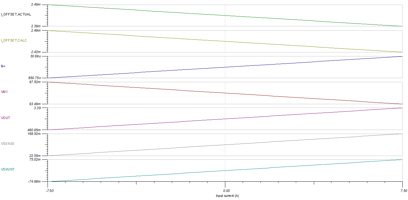
In this configuration, an error will occur as VSHUNT voltage increases. Note that the offset current is established via the difference between the supply voltage, and the voltage on the IN+ node as per Equation 6. IN+ is not a true 0 V, but will fluctuate as VSHUNT increases or decreases, resulting in additional error. INA901-SP Low Side Simulation Results shows simulated results and values for this design.
 Figure 2-2 INA901-SP Low-Side Simulation Results
Note that these curves are captured at ideal resistor values for R1 and R2, and resistor value tolerance, even at room temperature, will inject additional error between simulated and real results. The INA901 TINA-TI SPICE model also provides the ability to examine the input bias currents over load current range of the device.
From the TINA simulation data and schematic, a few constraints can be observed for this implementation:
- This topology cannot be implemented on the high side where VCM > VS, as the current must flow toward the IN+ pin to achieve the necessary offset. Therefore, the common-mode voltage of the IN+ pin must be less than that of the supply voltage to ensure valid operation.
- The offset current created by Equation 6 shows that, as a consequence, the offset voltage point deviates slightly with the sense voltage, producing a linear error along with the sense voltage.
- Because this is a low-side implementation, the trade-offs that come with measuring on the low side are in effect here. This includes the inability of the load to detect ground faults.
This design was then prototyped for real-world comparison. Table 2-1 through Table 2-3 display data captured via this topology at ambient temperature, as well as temperature extremes of –55°C and 125°C. For these data sets, E96 resistors of 0.1% tolerance were utilized, with a temperature coefficient of 50 ppm/°C. More tightly grouped curves may be obtained by choosing resistors with more stringent temperature drift specifications.
ILOAD (A) | VSHUNT, Meas. (V) | Output Voltage, Meas. Ideal (V) | VOUT, Meas. (V) | Error (%) | VOUT, | Error, |
|---|---|---|---|---|---|---|
–7.5 | –0.074997 | 0.46006 | 0.42527 | –7.56% | 0.45701 | –0.66% |
–6.25 | –0.062498 | 0.71004 | 0.67569 | –4.84% | 0.70743 | –0.37% |
–5 | –0.049998 | 0.96004 | 0.92612 | –3.53% | 0.95786 | –0.23% |
–3.75 | –0.037498 | 1.21004 | 1.17658 | –2.77% | 1.20832 | –0.14% |
–2.5 | –0.024998 | 1.46004 | 1.4271 | –2.26% | 1.45884 | –0.08% |
–1.25 | –0.012498 | 1.71004 | 1.6777 | –1.89% | 1.70944 | –0.04% |
0 | 0.000012 | 1.96024 | 1.9285 | –1.62% | 1.96024 | 0.00% |
1.25 | 0.012512 | 2.21024 | 2.1743 | –1.63% | 2.20604 | –0.19% |
2.5 | 0.025012 | 2.46024 | 2.42 | –1.64% | 2.45174 | –0.35% |
3.75 | 0.037511 | 2.71022 | 2.6657 | –1.64% | 2.69744 | –0.47% |
5 | 0.05001 | 2.9602 | 2.9115 | –1.65% | 2.94324 | –0.57% |
6.25 | 0.062513 | 3.21026 | 3.1573 | –1.65% | 3.18904 | –0.66% |
7.5 | 0.075012 | 3.46024 | 3.403 | –1.65% | 3.43474 | –0.74% |
ILOAD (A) | VSHUNT, Meas. (V) | Output Voltage, Meas. Ideal (V) | VOUT, Meas. (V) | Error (%) | VOUT, | Error, |
|---|---|---|---|---|---|---|
–7.5 | –0.074998 | 0.46004 | 0.43285 | –5.91% | 0.46459 | 0.99% |
–6.25 | –0.062498 | 0.71004 | 0.68348 | –3.74% | 0.71522 | 0.73% |
–5 | –0.049999 | 0.96002 | 0.93382 | –2.73% | 0.96556 | 0.58% |
–3.75 | –0.037498 | 1.21004 | 1.1842 | –2.14% | 1.21594 | 0.49% |
–2.5 | –0.024998 | 1.46004 | 1.4346 | –1.74% | 1.46634 | 0.43% |
–1.25 | –0.012498 | 1.71004 | 1.6849 | –1.47% | 1.71664 | 0.39% |
0 | –0.000002 | 1.95996 | 1.9353 | –1.26% | 1.96704 | 0.36% |
1.25 | 0.012506 | 2.21012 | 2.1815 | –1.29% | 2.21324 | 0.14% |
2.5 | 0.025006 | 2.46012 | 2.427 | –1.35% | 2.45874 | –0.06% |
3.75 | 0.037506 | 2.71012 | 2.6727 | –1.38% | 2.70444 | –0.21% |
5 | 0.050007 | 2.96014 | 2.9182 | –1.42% | 2.94994 | –0.34% |
6.25 | 0.062506 | 3.21012 | 3.1638 | –1.44% | 3.19554 | –0.45% |
7.5 | 0.075006 | 3.46012 | 3.4094 | –1.47% | 3.44114 | –0.55% |
ILOAD (A) | VSHUNT, Meas. (V) | Output Voltage, Meas. Ideal (V) | VOUT, Meas. (V) | Error (%) | VOUT, | Error, |
|---|---|---|---|---|---|---|
–7.5 | –0.074999 | 0.46002 | 0.42959 | –6.61% | 0.46133 | 0.28% |
–6.25 | –0.062498 | 0.71004 | 0.68015 | –4.21% | 0.71189 | 0.26% |
–5 | –0.049998 | 0.96004 | 0.93083 | –3.04% | 0.96257 | 0.26% |
–3.75 | –0.037498 | 1.21004 | 1.1815 | –2.36% | 1.21324 | 0.26% |
–2.5 | –0.024998 | 1.46004 | 1.4322 | –1.91% | 1.46394 | 0.27% |
–1.25 | –0.012498 | 1.71004 | 1.6829 | –1.59% | 1.71464 | 0.27% |
0 | 0.000006 | 1.96012 | 1.9339 | –1.34% | 1.96564 | 0.28% |
1.25 | 0.012506 | 2.21012 | 2.1798 | –1.37% | 2.21154 | 0.06% |
2.5 | 0.025006 | 2.46012 | 2.4257 | –1.40% | 2.45744 | –0.11% |
3.75 | 0.037505 | 2.7101 | 2.6715 | –1.42% | 2.70324 | –0.25% |
5 | 0.050006 | 2.96012 | 2.9174 | –1.44% | 2.94914 | –0.37% |
6.25 | 0.062506 | 3.21012 | 3.1632 | –1.46% | 3.19494 | –0.47% |
7.5 | 0.075007 | 3.46014 | 3.4092 | –1.47% | 3.44094 | –0.55% |
While this design allows bidirectional current sensing, the device remains a unidirectional device. This implies that one direction of sensing is more inaccurate than the other, as one direction drives the output stage towards its full scale range, where error is minimized against the gain error of the INA901, while the latter direction drives the device towards its referenced ground, and the inherent offset of the device applies additional error in this condition.
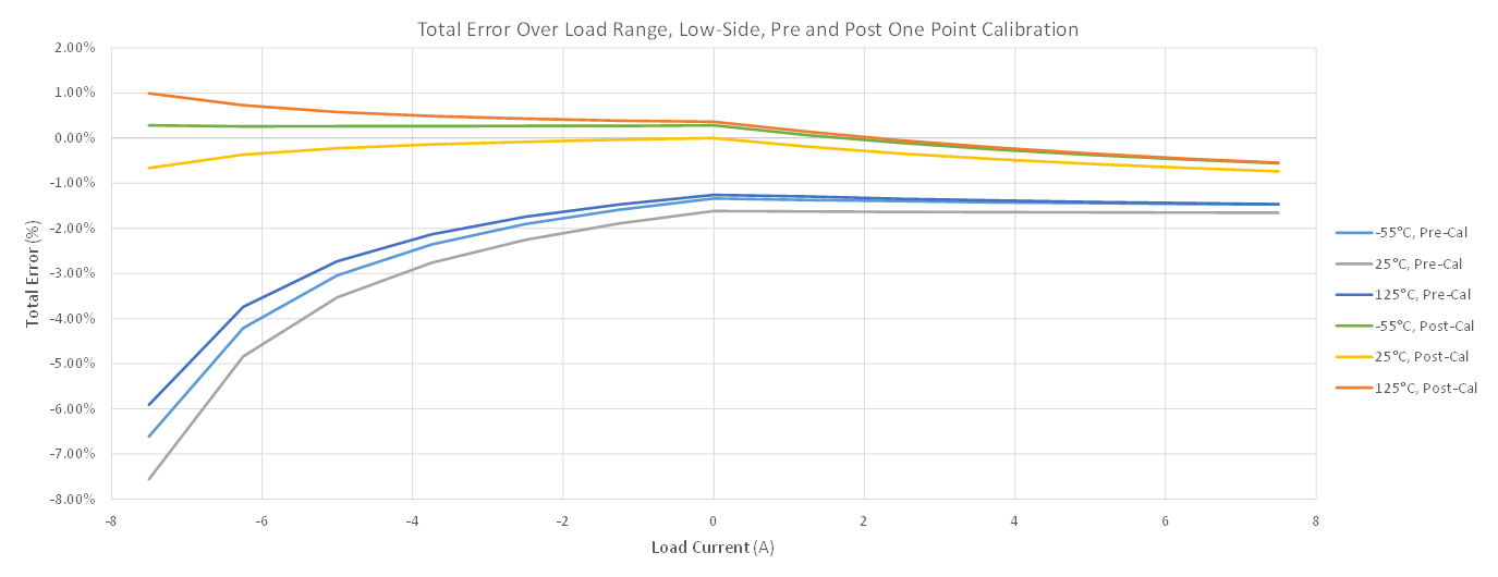
For use of such topologies, perform at least a one point calibration for optimal results. This is achieved in logic by capturing the true offset on the output created at the condition VSHUNT = 0 V, and shifting the output curve data down to this calculated offset point. Table 2-1 through Table 2-3 provide data points captured pre-calibration, as well as expected error pre- and post-calibration. Observe in Figure 2-3, that by performing calibration, error can be kept to 1% or less for the entirety of the measurement range. Resistors with additional drift specification may help achieve even better results.
 Figure 2-3 Low-Side, Bidirectional Error Over Range, Pre- and Post-Calibration