SBOA558 November 2022 LMH6642 , LMH6643 , LMH6643Q-Q1 , LMH6644 , OPA2328 , OPA328
3 ADC Driver Using OPAx328 High-Speed Op Amp
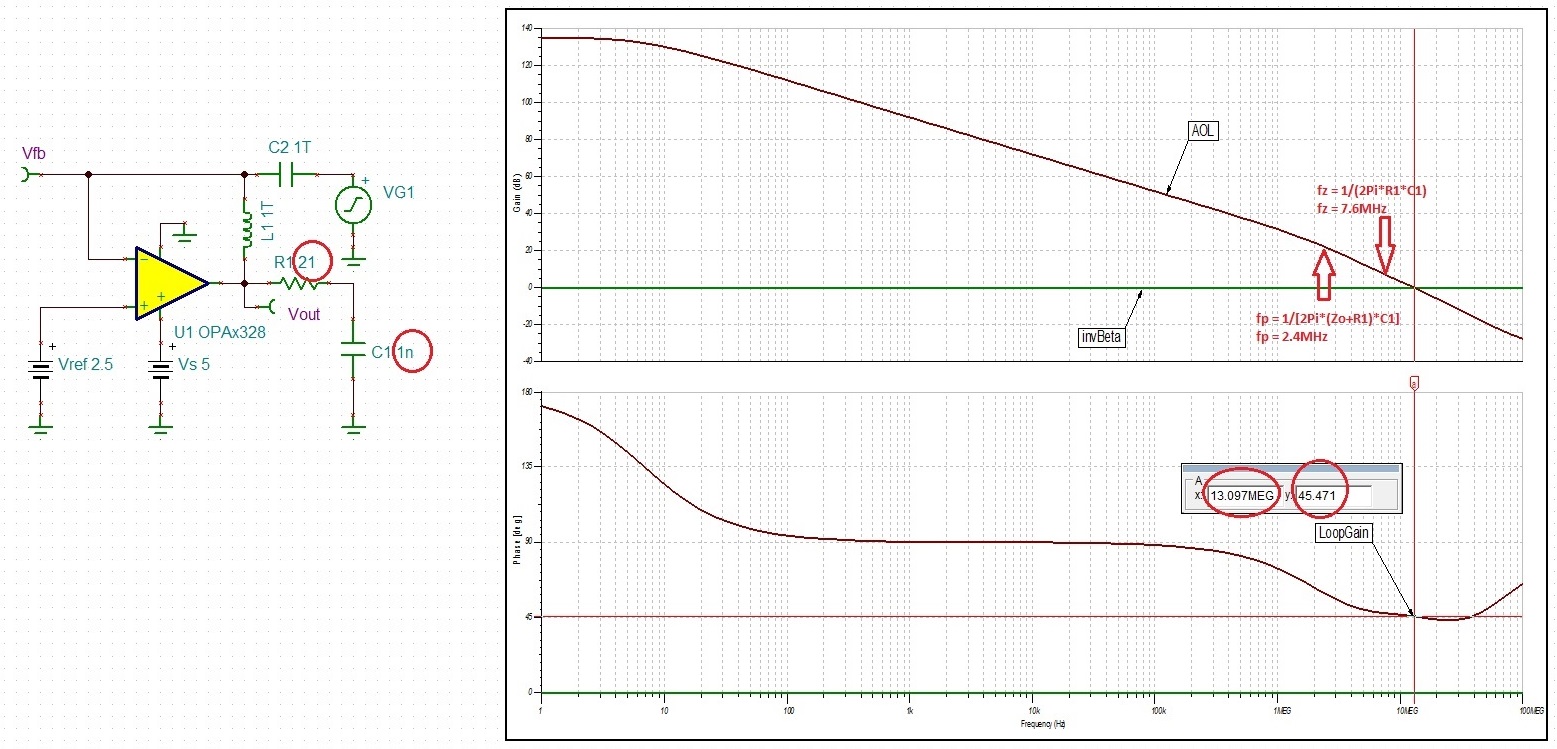 Figure 3-1 Stability Analysis of ADC
Driver Using OPAx328
Figure 3-1 Stability Analysis of ADC
Driver Using OPAx328Running a small-signal transient simulation of the OPAx328 buffer driving 1-nF capacitor with 21-Ω series output resistor, R1, confirms stable operation of the circuit, see Figure 3-2.
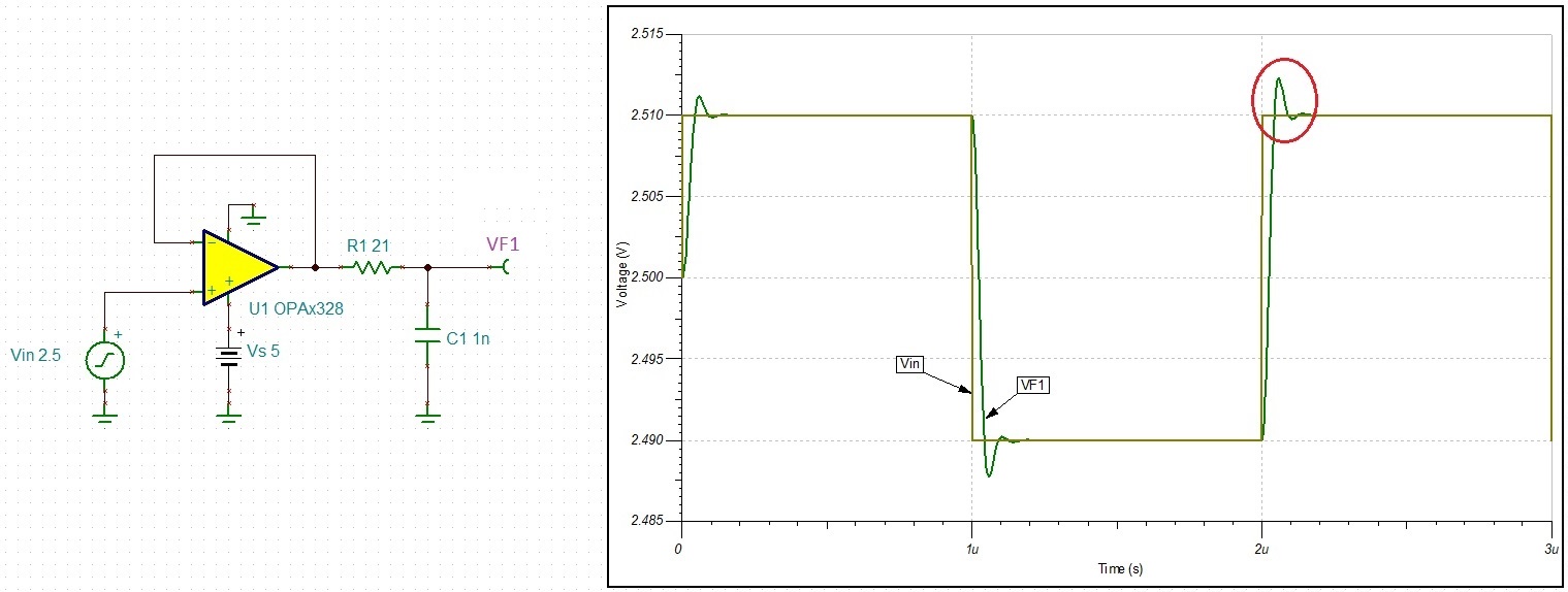 Figure 3-2 Transient Simulation of ADC
Driver Using OPAx328
Figure 3-2 Transient Simulation of ADC
Driver Using OPAx328However, if the output of the buffer amplifier includes a load resistor, RL, this creates a resistive divider between Riso and RL resistors that results in a gain error as shown in Figure 3-3. Thus, to eliminate the output voltage error, a dual feedback configuration might be used as shown in Figure 3-4.
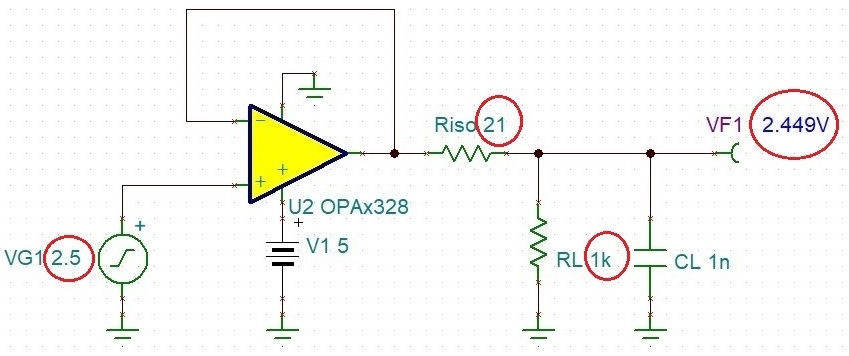 Figure 3-3 ADC Driver Gain Error Due
to Resistive Loading
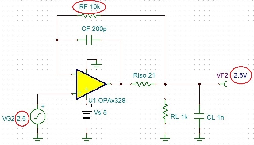 Figure 3-4 ADC Driver Dual Feedback
Using OPAx328
Figure 3-4 ADC Driver Dual Feedback
Using OPAx328The dual feedback configuration eliminates the output error with RF resistor driving the right side of the Riso resistor (thus controlling the DC output of the amplifier) while CF forms a buffer for AC signal by driving the left side of the Riso resistor, see Figure 3-5. This effectively duplicates fp/fz AC stability scheme employed in Figure 3-1 while eliminating DC output error caused by RL loading shown in Figure 3-3. The appropriate values of RF and CF need to be carefully determined to optimize the transient settling time.
 Figure 3-5 Dual Feedback ADC Driver
Stability Analysis Using OPAx328
Figure 3-5 Dual Feedback ADC Driver
Stability Analysis Using OPAx328As was the case shown in Figure 3-2, performing a small-signal transient analysis confirms stable operation of the circuit with minimum ringing and optimal settling time, see Figure 3-6.
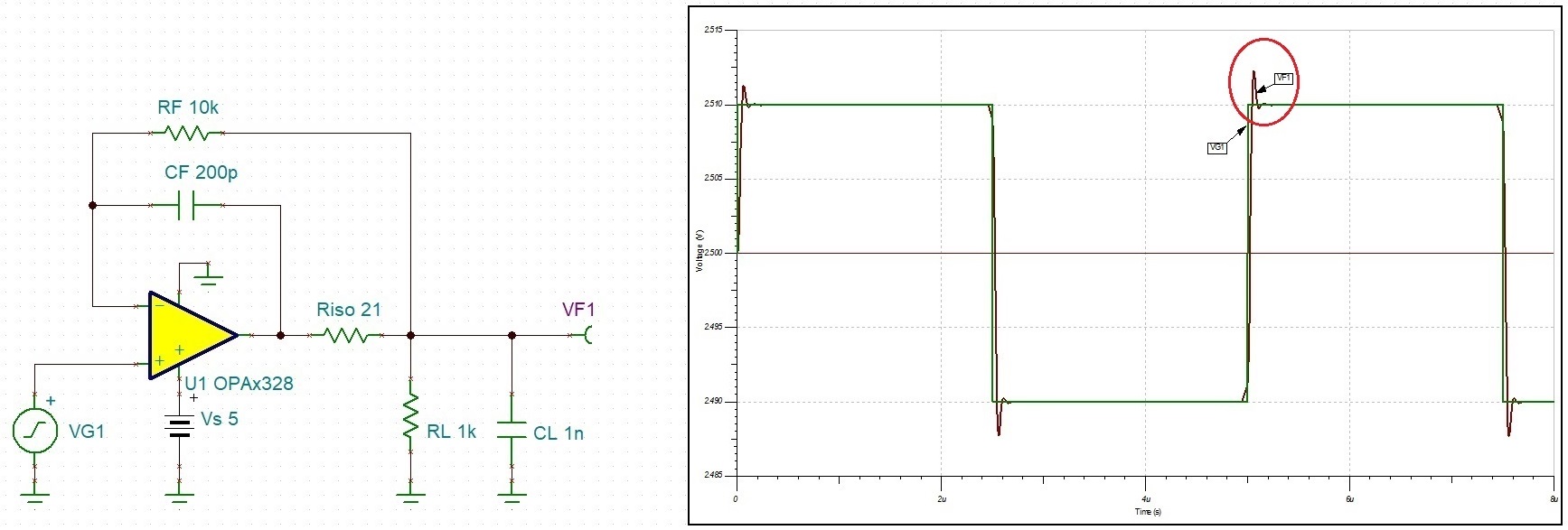 Figure 3-6 Dual Feedback ADC Driver
Transient Simulation Using OPAx328