SBOA615 November 2024 INA180 , INA180-Q1 , INA181 , INA181-Q1 , INA183 , INA185 , INA185-Q1 , INA186 , INA186-Q1 , INA190 , INA190-EP , INA190-Q1 , INA191 , INA199 , INA199-Q1 , INA209 , INA210 , INA210-Q1 , INA211 , INA211-Q1 , INA212 , INA212-Q1 , INA213 , INA213-Q1 , INA214 , INA214-Q1 , INA215 , INA215-Q1 , INA216 , INA2180 , INA2180-Q1 , INA2181 , INA2181-Q1 , INA219 , INA2191 , INA220 , INA220-Q1 , INA223 , INA225 , INA225-Q1 , INA226 , INA226-Q1 , INA228 , INA228-Q1 , INA229 , INA229-Q1 , INA2290 , INA230 , INA231 , INA232 , INA233 , INA234 , INA236 , INA237 , INA237-Q1 , INA238 , INA238-Q1 , INA239 , INA239-Q1 , INA240 , INA240-Q1 , INA241A , INA241A-Q1 , INA241B , INA241B-Q1 , INA250 , INA250-Q1 , INA253 , INA253-Q1 , INA254 , INA260 , INA280 , INA280-Q1 , INA281 , INA281-Q1 , INA290 , INA290-Q1 , INA293 , INA293-Q1 , INA296A , INA296A-Q1 , INA296B , INA296B-Q1 , INA300 , INA300-Q1 , INA301 , INA301-Q1 , INA302 , INA302-Q1 , INA303 , INA303-Q1 , INA310A , INA310A-Q1 , INA310B , INA310B-Q1 , INA3221 , INA3221-Q1 , INA381 , INA381-Q1 , INA4180 , INA4180-Q1 , INA4181 , INA4181-Q1 , INA4230 , INA4235 , INA4290 , INA700 , INA740A , INA740B , INA745A , INA745B , INA780A , INA780B , INA790B , INA791B , LMP8278Q-Q1 , LMP8601 , LMP8601-Q1 , LMP8602 , LMP8602-Q1 , LMP8603 , LMP8603-Q1 , LMP8640 , LMP8640-Q1 , LMP8640HV
- 1
- Abstract
- Trademarks
- 1Introduction
- 2What is ESD, EOS, and Latch Up?
- 3Risky Applications for Current Sense Amplifiers
- 4Summary
- 5References
3.1 Applications with Over Voltage Transient Surges (EOS)
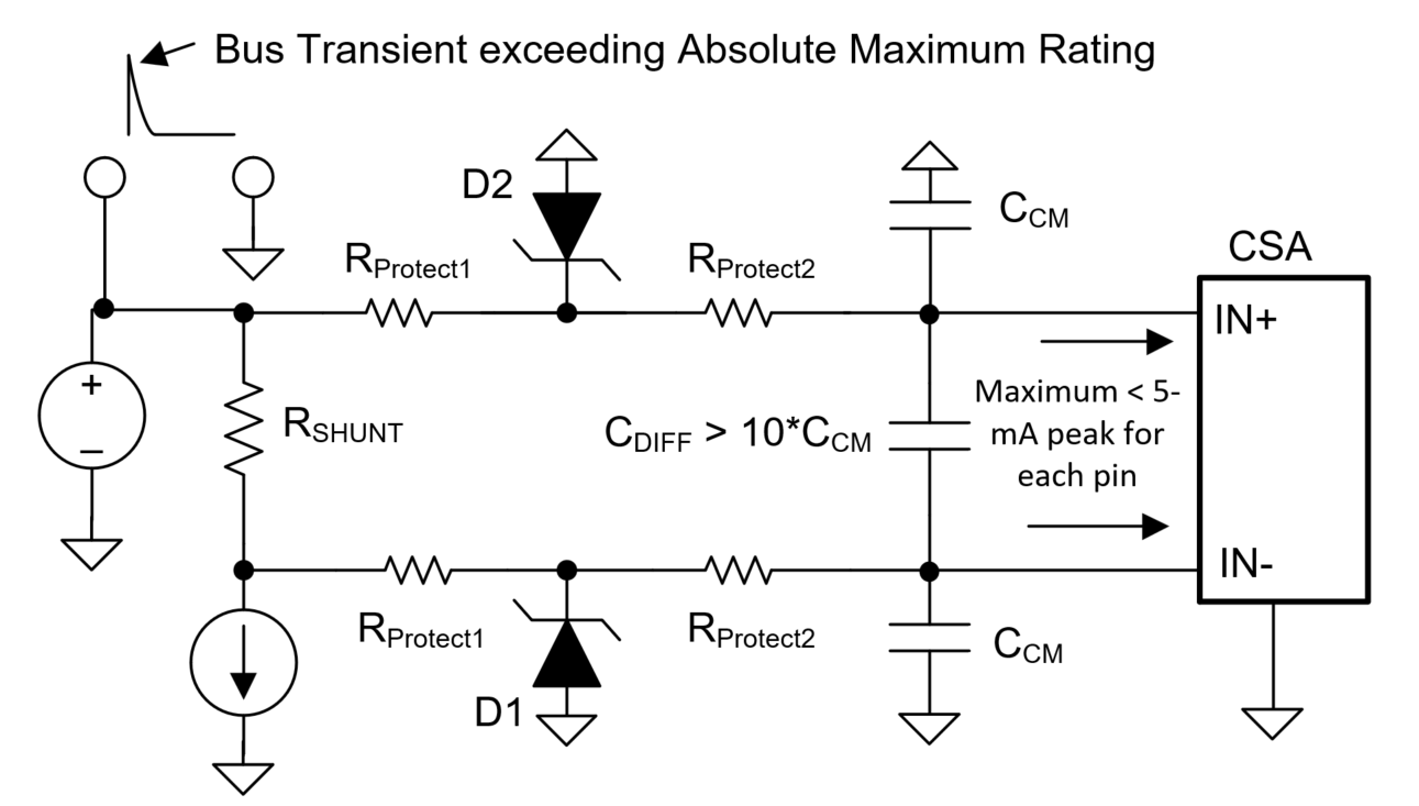
For applications where input voltages can exceed input ratings, the easiest option is to choose a CSA (or even a hall-based or isolated current sensor) that can survive the voltage; however, this is not always possible. When this is the case, the best practice is to use the following input protection scheme shown in Figure 3-1.
 Figure 3-1 Input Protection for
EOS
Figure 3-1 Input Protection for
EOSIn Figure 3-1, D1 and D2 need reverse-breakdown voltages before the Absolute Maximum VCM Voltage of the CSA. Ideally, voltages at input pins are clamped before the maximum VCM rating. If D1 and D2 clamp after the VCM rating, the RProtect2 resistor can limit the rest of current into ESD pin to < 5mA peak. General equation to determine RProtect2 is shown in Equation 1.
Figure 3-1 shows unidirectional diodes and not bidirectional TVS diodes because during negative voltage event the clamping diodes breakdown with their forward bias characteristic, which is much better than a larger breakdown voltage. The resulting forward bias voltage (VF) can probably be less than the -0.3V minimum VCM rating for low-side CSAs. Thus, for negative voltage surges, RProtect2 can be necessary to still limit current according to Equation 2.
If the CSA is going to be rated to system level standards such as IEC61000-4-2, then D1 and D2 need to be TVS diodes. For any less stringent and/or slower EOS events, D1 and D2 can be Zener diodes that are rated to withstand the current draw for however long the EOS can occur. It is best to conservatively assume that the EOS condition can last indefinitely.
RProtect1 helps limit current mostly into D1 and D2 (and thus reduces required power ratings). However, there can be a tradeoff with circuit offset error over temperature due to D1 and D2 leakage currents. Mismatch in these leakage currents, along with mismatch in the RProtect1 resistors can create variable voltage drops in the RProtect1 resistors, which can cause input offset error.
The input capacitors (CCM and CDIFF) can attenuate fast voltage surges increase robustness to system level testing and noise immunity.
Most CSAs (except for high-input impedance ones such as INA190 or INA186) can require total resistance into an input (RProtect1+RProtect2) to be less than 10-Ohm to avoid any noticeable change in error. However, there are methods to bound this error. Refer to this Input Resistance Error for Current Sense Amplifiers, user's guide for more information.
Additional testing of a CSA against IEC surges can be found Transient Robustness for Current Shunt Monitor, reference design.