SBOS424C March 2008 – November 2015 PGA112 , PGA113 , PGA116 , PGA117
PRODUCTION DATA.
- 1 Features
- 2 Applications
- 3 Description
- 4 Revision History
- 5 Device Comparison
- 6 Pin Configuration and Functions
- 7 Specifications
- 8 Detailed Description
-
9 Applications and Implementation
- 9.1
Application Information
- 9.1.1 Op Amp: Input Stage
- 9.1.2 Op Amp: General Gain Equations
- 9.1.3 Op Amp: Frequency Response Versus Gain
- 9.1.4 Analog MUX
- 9.1.5 System Calibration Using The PGA
- 9.1.6 Driving and Interfacing to ADCs
- 9.1.7 Power Supplies
- 9.1.8 Shutdown and Power-On-Reset (POR)
- 9.1.9 Typical Connections: PGA116, PGA117 (TSSOP-20)
- 9.2 Typical Applications
- 9.1
Application Information
- 10Power Supply Recommendations
- 11Layout
- 12Device and Documentation Support
- 13Mechanical, Packaging, and Orderable Information
9 Applications and Implementation
NOTE
Information in the following applications sections is not part of the TI component specification, and TI does not warrant its accuracy or completeness. TI’s customers are responsible for determining suitability of components for their purposes. Customers should validate and test their design implementation to confirm system functionality.
9.1 Application Information
The PGA11x family of devices are single-ended input, single-supply, programmable gain amplifiers (PGAs) with an input multiplexer. Multiplexer channel selection and gain selection are done through a standard SPI interface. The PGA112 and PGA113 have a two-channel input MUX and the PGA116 and PGA117 devices have a 10-channel input MUX. The PGA112 and PGA116 devices provide binary gain selections (1, 2, 4, 8, 16, 32, 64, 128) and the PGA113 and PGA117 devices provide scope gain selections (1, 2, 5, 10, 20, 50, 100, 200). All models use a split-supply architecture with an analog supply, AVDD, and a digital supply, DVDD. This split-supply architecture allows for ease of interface to analog-to-digital converters (ADCs) and microcontrollers in mixed-supply voltage systems, such as where the analog supply is 5 V and the digital supply is 3 V. Four internal calibration channels are provided for system-level calibration. The channels are tied to GND, 0.9 VCAL, 0.1 VCAL, and VREF, respectively. VCAL, an external voltage connected to VCAL/CH0, acts as the system calibration reference. If VCAL is the system ADC reference, then gain and offset calibration on the ADC are easily accomplished through the PGA11x devices using only one MUX input. If calibration is not used, then VCAL/CH0 can be used as a standard MUX input. All four versions provide a VREF pin that can be tied to ground or, for ease of scaling, to midsupply in single-supply systems where midsupply is used as a virtual ground. The PGA112 and PGA113 devices offer a software-controlled shutdown feature for low standby power. The PGA116 and PGA117 devices offer both hardware- and software-controlled shutdown for low standby power. The PGA112 and PGA113 devices have a 3-wire SPI digital interface; the PGA116 and PGA117 devices have a four-wire SPI digital interface. The PGA116 and PGA117 devices also have daisy-chain capability.
9.1.1 Op Amp: Input Stage
The PGA op amp is a rail-to-rail input and output (RRIO) single-supply op amp. The input topology uses two separate input stages in parallel to achieve rail-to-rail input. As Figure 66 shows, there is a PMOS transistor on each input for operation down to ground; there is also an NMOS transistor on each input in parallel for operation to the positive supply rail. When the common-mode input voltage (that is, the single-ended input, because this PGA is configured internally for noninverting gain) crosses a level that is typically about 1.5 V less than the positive supply, there is a transition between the NMOS and PMOS transistors. The result of this transition appears as a small input offset voltage transition that is reflected to the output by the selected PGA gain. This transition may be either increasing or decreasing, and differs from part to part as described in Figure 67 and Figure 68. These figures illustrate possible differences in input offset voltage between two different devices when used with AVDD = 5 V. Because the exact transition region varies from device to device, the Electrical Characteristics: VS = AVDD = DVDD = 5 V table specifies an input offset voltage above and below this input transition region.
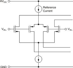 Figure 66. PGA Rail-To-Rail Input Stage
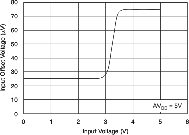 Figure 67. VOS Versus Input Voltage—Case 1
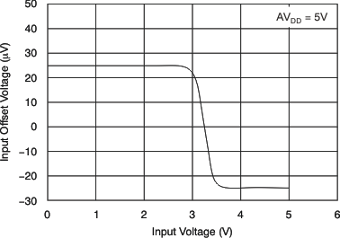 Figure 68. VOS Versus Input Voltage—Case 2
9.1.2 Op Amp: General Gain Equations
Figure 69 shows the basic configuration for using the PGA as a gain block. VOUT / VIN is the selected noninverting gain, depending on the model selected, for either binary or scope gains.
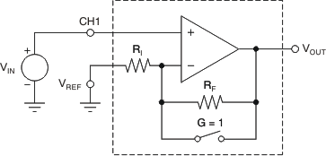 Figure 69. PGA Used as a Gain Block

where
- G = 1, 2, 4, 8, 16, 32, 64, and 128 (binary gains)
- G = 1, 2, 5, 10, 20, 50, 100, and 200 (scope gains)
Figure 70 shows the PGA configuration and gain equations for VREF = AVDD/2. VOUT0 is VOUT when CH0 is selected and VOUT1 is VOUT when CH1 is selected. Notice the VREF pin has no effect for G = 1 because the internal feedback resistor, RF, is shorted out. This configuration allows for positive and negative voltage excursions around a midsupply virtual ground.
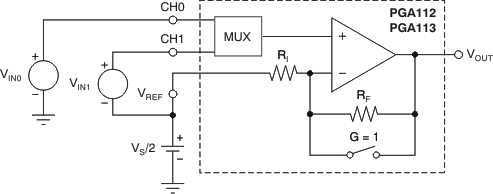 Figure 70. PGA112 and PGA113 Configuration for Positive and Negative Excursions Around Midsupply Virtual Ground

When: G = 1
Then: VOUT0 = G × VIN0

where
- G = 1, 2, 4, 8, 16, 32, 64, and 128 (binary gains)
- G = 1, 2, 5, 10, 20, 50, 100, and 200 (scope gains)
Table 7 details the internal typical values for the op amp internal feedback resistor (RF) and op amp internal input resistor (RI) for both binary and scope gains.
Table 7. Typical RF and RI Versus Gain
| BINARY GAIN (V/V) | RF (Ω) | RI (Ω) | SCOPE GAIN (V/V) | RF (Ω) | RI (Ω) | |
|---|---|---|---|---|---|---|
| 1 | 0 | 3.25 k | 1 | 0 | 3.25 k | |
| 2 | 3.25 k | 3.25 k | 2 | 3.25 k | 3.25 k | |
| 4 | 9.75 k | 3.25 k | 5 | 13 k | 3.25 k | |
| 8 | 22.75 k | 3.25 k | 10 | 29.25 k | 3.25 k | |
| 16 | 48.75 k | 3.25 k | 20 | 61.75 k | 3.25 k | |
| 32 | 100.75 k | 3.25 k | 50 | 159.25 k | 3.25 k | |
| 64 | 204.75 k | 3.25 k | 100 | 321.75 k | 3.25 k | |
| 128 | 412.75 k | 3.25 k | 200 | 646.75 k | 3.25 k |
9.1.3 Op Amp: Frequency Response Versus Gain
Table 8 documents how small-signal bandwidth and slew rate change correspond to changes in PGA gain.
Full power bandwidth (that is, the highest frequency that a sine wave can pass through the PGA for a given gain) is related to slew rate by Equation 4:

where
- SR = Slew rate in V/μs
- f = Frequency in Hz
- VOP = Output peak voltage in volts
9.1.3.1 Example:
For G = 8, then SR = 10.6 V/μs (slew rate rise is minimum slew rate).
For a 5-V system, choose 0.1 V < VOUT < 4.9 V or VOUTPP = 4.8 V or VOUTP = 2.4 V.
SR (V/μs) = 2πf × VOP (1 × 10⁻⁶).
10.6 = 2πf (2.4) (1 × 10⁻⁶) → f = 702.9 kHz
This example shows that a G = 8 configuration can produce a 4.8-VPP sine wave with frequency up to 702.9 kHz. This computation only shows the theoretical upper limit of frequency for this example, but does not indicate the distortion of the sine wave. The acceptable distortion depends on the specific application. As a general guideline, maintain two to three times the calculated slew rate to minimize distortion on the sine wave. For this example, the application should only use G = 8, 4.8 VPP, up to a frequency range of 234 kHz to 351 kHz, depending upon the acceptable distortion. For a given gain and slew rate requirement, check for adequate small-signal bandwidth (typical –3-dB frequency) to assure that the frequency of the signal can be passed without attenuation.
9.1.4 Analog MUX
The analog input MUX provides two input channels for the PGA112 and PGA113 devices and 10 input channels for the PGA116 and PGA117 devices. The MUX switches are designed to be break-before-make and thereby eliminate any concerns about shorting the two input signal sources together.
Four internal MUX CAL channels are included in the analog MUX for ease of system calibration. These CAL channels allow ADC gain and offset errors to be calibrated out. This calibration does not remove the offset and gain errors of the PGA for gains greater than 1, but most systems should see a significant increase in the ADC accuracy. In addition, these CAL channels can be used by the ADC to read the minimum and maximum possible voltages from the PGA. With these minimum and maximum levels known, the system architecture can be designed to indicate an out-of-range condition on the measured analog input signals if these levels are ever measured.
To use the CAL channels, VCAL/CH0 must be permanently connected to the system ADC reference. There is a typical 100-kΩ load from VCAL/CH0 to ground. Table 9 illustrates how to use the CAL channels with VREF = ground. Table 10 describes how to use the CAL channels with VREF = AVDD/2. The VREF pin must be connected to a source that is low-impedance for both DC and AC to maintain gain and nonlinearity accuracy. Worst-case current demand on the VREF pin occurs when G = 1 because there is a 3.25-kΩ resistor between VOUT and VREF. For a 5-V system with AVDD/2 = 2.5 V, the VREF pin buffer must source and sink 2.5 V/3.25 kΩ = 0.7 mA minimum for a VOUT that can swing from ground to 5 V.
Table 8. Frequency Response versus Gain (CL = 100 pf, RL= 10 kω)
| BINARY GAIN (V/V) | TYPICAL –3dB FREQUENCY (MHz) |
SLEW RATE-FALL (V/μs) |
SLEW RATE-RISE (V/μs) |
0.1% SETTLING TIME: 4VPP (μs) |
0.01% SETTLING TIME: 4VPP (μs) |
SCOPE GAIN (V/V) |
TYPICAL –3dB FREQUENCY (MHz) |
SLEW RATE-FALL (V/μs) |
SLEW RATE-RISE (V/μs) |
0.1% SETTLING TIME: 4VPP (μs) |
0.01% SETTLING TIME: 4VPP (μs) |
|
|---|---|---|---|---|---|---|---|---|---|---|---|---|
| 1 | 10 | 8 | 3 | 2 | 2.55 | 1 | 10 | 8 | 3 | 2 | 2.55 | |
| 2 | 3.8 | 9 | 6.4 | 2 | 2.6 | 2 | 3.8 | 9 | 6.4 | 2 | 2.6 | |
| 4 | 2 | 12.8 | 10.6 | 2 | 2.6 | 5 | 1.8 | 12.8 | 10.6 | 2 | 2.6 | |
| 8 | 1.8 | 12.8 | 10.6 | 2 | 2.6 | 10 | 1.8 | 12.8 | 10.6 | 2.2 | 2.6 | |
| 16 | 1.6 | 12.8 | 12.8 | 2.3 | 2.6 | 20 | 1.3 | 12.8 | 9.1 | 2.3 | 2.8 | |
| 32 | 1.8 | 12.8 | 13.3 | 2.3 | 3 | 50 | 0.9 | 9.1 | 7.1 | 2.4 | 3.8 | |
| 64 | 0.6 | 4 | 3.5 | 3 | 6 | 100 | 0.38 | 4 | 3.5 | 4.4 | 7 | |
| 128 | 0.35 | 2.5 | 2.5 | 4.8 | 8 | 200 | 0.23 | 2.3 | 2 | 6.9 | 10 |
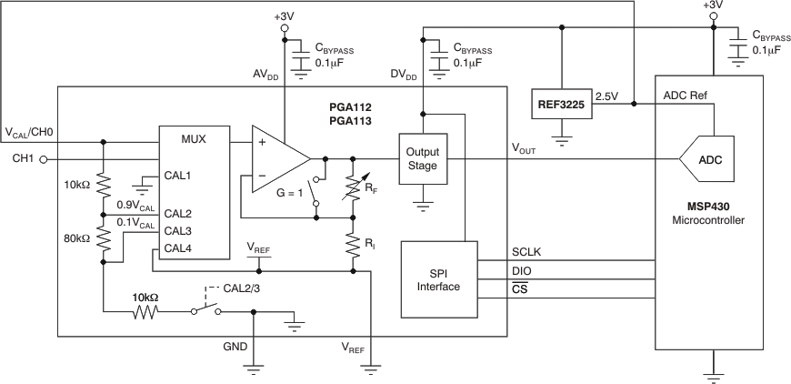 Figure 71. Using CAL Channels With VREF = Ground
Table 9. Using the MUX CAL Channels With VREF = GND
(AVDD = 3 V, DVDD = 3 V, ADC Ref = 2.5 V, and VREF = GND)
| FUNCTION | MUX SELECT | GAIN SELECT | MUX INPUT | OP AMP (+In) |
OP AMP (VOUT) |
DESCRIPTION |
|---|---|---|---|---|---|---|
| Minimum Signal | CAL1 | 1 | GND | GND | 50 mV | Minimum signal level that the MUX, op amp, and ADC can read. Op amp VOUT is limited by negative saturation. |
| Gain Calibration | CAL2 | 1 | 0.9 × (VCAL/CH0) | 2.25 V | 2.25 V | 90% ADC Ref for system full-scale or gain calibration of the ADC. |
| Maximum Signal | CAL2 | 2 | 0.9 × (VCAL/CH0) | 2.25 V | 2.95 V | Maximum signal level that the MUX, op amp, and ADC can read. Op amp VOUT is limited by positive saturation. System is limited by ADC max input of 2.5 V (ADC Ref = 2.5 V). |
| Offset Calibration | CAL3 | 1 | 0.1 × (VCAL/CH0) | 0.25 V | 0.25 V | 10% ADC Ref for system offset calibration of the ADC. |
| Minimum Signal | CAL4 | 1 | VREF | GND | 50 mV | Minimum signal level that the MUX, op amp, and ADC can read. Op amp VOUT is limited by negative saturation. |
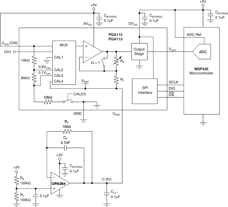 Figure 72. Using CAL Channels With VREF = AVDD/2
Table 10. Using the MUX CAL Channels With VREF = AVDD/2
(AvDD = 3 V, DVDD = 3 V, ADC Ref = 3 V, and VREF = 1.5 V)
| FUNCTION | MUX SELECT | GAIN SELECT | MUX INPUT | OP AMP (+In) |
OP AMP (VOUT) |
DESCRIPTION |
|---|---|---|---|---|---|---|
| Minimum Signal | CAL1 | 1 | GND | GND | 50 mV | Minimum signal level that the MUX, op amp, and ADC can read. Op amp VOUT is limited by negative saturation. |
| Gain Calibration | CAL2 | 1 | 0.9 × (VCAL/CH0) | 2.7 V | 2.7 V | 90% ADC Ref for system full-scale or gain calibration of the ADC. |
| Maximum Signal | CAL2 | 4 or 5 | 0.9 × (VCAL/CH0) | 2.25 V | 2.95 V | Maximum signal level that the MUX, op amp, and ADC can read. Op amp VOUT is limited by positive saturation. |
| Offset Calibration | CAL3 | 1 | 0.1 × (VCAL/CH0) | 0.3 V | 0.3 V | 10% ADC Ref for system offset calibration of the ADC. |
| VREF Check | CAL4 | 1 | VREF | 1.5 V | 1.5 V | Midsupply voltage used as VREF. |
9.1.5 System Calibration Using The PGA
Analog-to-digital converters (ADCs) contain two major errors that can be easily removed by calibration at a system level. These errors are gain error and offset error, as shown in Figure 73. Figure 73 shows a typical transfer function for a 12-bit ADC. The analog input is on the x-axis with a range from 0 V to (VREF_ADC – 1LSB), where VREF_ADC is the ADC reference voltage. The y-axis is the hexadecimal equivalent of the digital codes that result from ADC conversions. The dotted red line represents an ideal transfer function with 0000h representing 0 V analog input and 0FFFh representing an analog input of (VREF_ADC – 1LSB). The solid blue line illustrates the offset error. Although the solid blue line includes both offset error and gain error, at an analog input of 0 V the offset error voltage, VZ_ACTUAL, can be measured. The dashed black line represents the transfer function with gain error. The dashed black line is equivalent to the solid blue line without the offset error, and can be measured and computed using VZ_ACTUAL and VZ_IDEAL. The difference between the dashed black line and the dotted red line is the gain error. Gain and offset error can be computed by taking zero input and full-scale input readings. Using these error calculations, compute a calibrated ADC reading to remove the ADC gain and offset error.
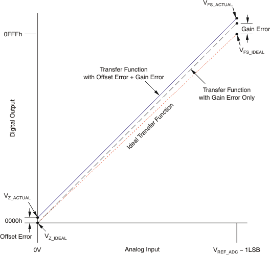 Figure 73. ADC Offset and Gain Error
In practice, the zero input (0 V) or full-scale input (VREF_ADC – 1LSB) of ADCs cannot always be measured because of internal offset error and gain error. However, if measurements are made very close to the full-scale input and the zero input, both zero and full-scale can be calibrated very accurately with the assumption of linearity from the calibration points to the desired end points of the ADC ideal transfer function. For the zero calibration, choose 10%VREF_ADC; this value should be above the internal offset error and sufficiently out of the noise floor range of the ADC. For the gain calibration, choose 90%VREF_ADC; this value should be less than the internal gain error and sufficiently below the tolerance of VREF. These key points can be summarized in this way:
For zero calibration:
- The ADC cannot read the ideal zero because of offset error
- Must be far enough above ground to be above noise floor and ADC offset error
- Therefore, choose 10%VREF_ADC for zero calibration
For gain calibration:
- The ADC cannot read the ideal full-scale because of gain error
- Must be far enough below full-scale to be below the VREF tolerance and ADC gain error
- Therefore, choose 90%VREF_ADC for gain calibration
The 12-bit ADC example in Figure 74 illustrates the technique for calibrating an ADC using a 10%VREF_ADC and 90%VREF_ADC reading where VREF_ADC is the ADC reference voltage. The 10%VREF reading also contains a gain error because it is not a VIN = 0 calibration point. First, use the 90%VREF and 10%VREF points to compute the measured gain error. The measured gain error is then used to remove the gain error from the 10%VREF reading, giving a measured 10%VREF number. The measured 10%VREF number is used to compute the measured offset error.
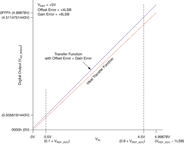 Figure 74. 12-Bit Example of ADC Calibration for Gain and Offset Error
The gain error and offset error in ADC readings can be calibrated by using 10%VREF_ADC and 90%VREF_ADC calibration points. Because the calibration is ratiometric to VREF_ADC, the exact value of VREF_ADC does not need to be known in the end application.
Follow these steps to compute a calibrated ADC reading:
- Take the ADC reading at VIN = 90% × VREF and VIN = 10% × VREF. The ADC readings for 10%VREF and 90%VREF are taken.
- Compute the ADC measured gain. The slope of the curve connecting the measured 10%VREF and measured 90%VREF point is computed and compared to the slope between the ideal 10%VREF and ideal 90%VREF. This result is the measured gain.
- Compute the ADC measured offset. The measured offset is computed by taking the difference between the measured 10%VREF and the (ideal 10%VREF) × (measured gain).
- Compute the calibrated ADC readings.


Any ADC reading can therefore be calibrated by removing the gain error and offset error. The measured offset is subtracted from the ADC reading and then divided by the measured gain to give a corrected reading. If this calibration is performed on a timed basis, relative to the specific application, gain and offset error over temperature are also removed from the ADC reading by calibration.
For example; given:
- 12-Bit ADC
- ADC Gain Error = 6 LSB
- ADC Offset Error = 4 LSB
- ADC Reference (VREF_ADC) = 5 V
- Temperature = 25°C
Table 11 shows the resulting system accuracy.
Table 11. Bits of System Accuracy(1) (To 0.5 LSB)
| VIN | ADC ACCURACY WITHOUT CALIBRATION | ADC ACCURACY WITH PGA112 CALIBRATION |
|---|---|---|
| 10%VREF_ADC | 8.80 Bits | 12.80 Bits |
| 90%VREF_ADC | 7.77 Bits | 11.06 Bits |
9.1.6 Driving and Interfacing to ADCs
CDAC SAR ADCs contain an input sampling capacitor, CSH, to sample the input signal during a sample period as shown in Figure 75. After the sample period, CSH is removed from the input signal. Subsequent comparisons of the charge stored on CSH are performed during the ADC conversion process. To achieve optimal op amp stability, input signal settling, and the demands for charge from the input signal conditioning circuitry, most ADC applications are optimized by the use of a resistor (RFILT) and capacitor (CFILT) filter placed between the op amp output and ADC input. For the PGA112 and PGA113 devices, or the PGA116 and PGA117 devices, setting CFILT = 1 nF and RFILT = 100 Ω yields optimum system performance for sampling converters operating at speeds up to 500 kHz, depending upon the application settling time and accuracy requirements.
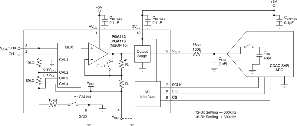 Figure 75. Driving and Interfacing to ADCs
9.1.7 Power Supplies
Figure 76 shows a typical mixed-supply voltage system where the analog supply, AVDD, is 5 V and the digital supply voltage, DVDD, is 3 V. The analog output stage of the PGA and the SPI interface digital circuitry are both powered from DVDD. When considering the power required for DVDD, use the Electrical Characteristics: VS = AVDD = DVDD = 5 V table and add any load current anticipated on VOUT; this load current must be provided by DVDD. This split-supply architecture ensures compatible logic levels with the microcontroller. It also ensures that the PGA output cannot run the input for the onboard ADC into an overvoltage condition; this condition could cause device latch-up and system lock-up, and require power-supply sequencing. Each supply pin should be individually bypassed with a 0.1 μF ceramic capacitor directly at the device to ground. If there is only one power supply in the system, AVDD and DVDD can both be connected to the same supply; however, TI recommends using individual bypass capacitors directly at each respective supply pin to a single point ground. VOUT is diode-clamped to AVDD (as shown in Figure 76); therefore, set DVDD less than or equal to AVDD + 0.3 V. DVDD and AVDD must be within the operating voltage range of 2.2 V to 5.5 V.
At initial power-on, the state of the PGA is G = 1 and Channel 0 active.
NOTE
For most applications, set AVDD ≥ DVDD to prevent VOUT from driving current into AVDD and raising the voltage level of AVDD
9.1.8 Shutdown and Power-On-Reset (POR)
The PGA112 and PGA113 devices have a software shutdown mode, and the PGA116 and PGA117 devices offer both a hardware and software shutdown mode. When the PGA11x is shut down, it goes into a low-power standby mode. The Electrical Characteristics: VS = AVDD = DVDD = 5 V table details the current draw in shutdown mode with and without the SPI interface being clocked. In shutdown mode, RF and RI remain connected between VOUT and VREF.
When DVDD is less than 1.6 V, the digital interface is disabled and the channel and gain selections are held to the respective POR states of Gain = 1 and Channel = VCAL/CH0. When DVDD is above 1.8 V, the digital interface is enabled and the POR gain and channel states remain unchanged until a valid SPI communication is received.
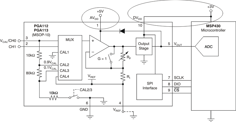 Figure 76. Split Power-Supply Architecture: AVDD ≠ DvDD
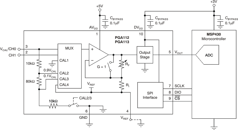 Figure 77. PGA112, PGA113 (VSSOP-10) Typical Application Schematic
9.1.9 Typical Connections: PGA116, PGA117 (TSSOP-20)
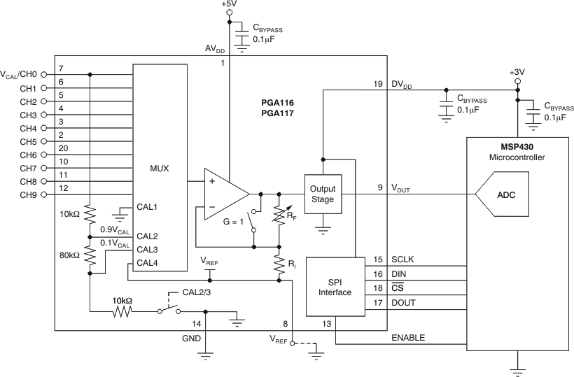 Figure 78. PGA116, PGA117 (TSSOP-20)
9.2 Typical Applications
9.2.1 Bipolar Input to Single-Supply Scaling
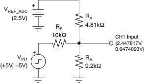 Figure 79. Bipolar to Single-Ended Input Algorithm
9.2.1.1 Design Requirements
Table 12. Bipolar to Single-Ended Input Scaling(1)(2)
| VREF_ADC (V) | VIN1 (V) | CH1 INPUT | RA (kΩ) | RX (Ω) | RB (kΩ) |
|---|---|---|---|---|---|
| 2.5 | –5 | 0.047613 | 9.2 | 4.81 k | 10 |
| 0 | 1.247613 | ||||
| 5 | 2.447613 | ||||
| 2.5 | –10 | 0.050317 | 3.16 | 2.4 k | 10 |
| 0 | 1.250317 | ||||
| 10 | 2.450317 | ||||
| 3 | –5 | 0.058003 | 13.5 | 5.76 k | 10 |
| 0 | 1.498003 | ||||
| 5 | 2.938003 | ||||
| 3 | –10 | 0.059303 | 4.02 | 2.87 k | 10 |
| 0 | 1.499303 | ||||
| 10 | 2.939303 | ||||
| 4.096 | –5 | 0.082224 | 37 | 7.87 k | 10 |
| 0 | 2.048304 | ||||
| 5 | 4.014384 | ||||
| 4.096 | –10 | 0.086018 | 6.49 | 3.92 k | 10 |
| 0 | 2.052098 | ||||
| 10 | 4.018178 | ||||
| 5 | –5 | 0.093506 | 24 | 965 | 10 |
| 0 | 2.493506 | ||||
| 5 | 4.893506 | ||||
| 5 | –10 | 0.095227 | 9.2 | 4.81 k | 10 |
| 0 | 2.495227 | ||||
| 10 | 4.895227 |
9.2.1.2 Detailed Design Procedure
This process assumes a symmetrical VIN1 and that symmetrical scaling is used for CH1 input minimum and maximum values. The following steps give the algorithm to compute resistor values for references not listed in Table 12.
Step 1: Choose the following:
- VREF_ADC = 2.5 V (ADC reference voltage)
- | VIN1 | = 5
- Choose RB as a standard resistor value. The input on-channel current multiplied by RB should be less than the input offset voltage, such that RB is not a major source of inaccuracy.
- For the most negative VIN1, choose the percentage (in decimal format) of VREF_ADC desired at the ADC input.
- For the most positive VIN1, choose the percentage (in decimal format) of VREF_ADC desired at the ADC input. Because this scaling is based on symmetry, kVO+ must be the same percentage away from VREF_ADC at the upper limit as at the lower limit where kVO– is computed.
(magnitude of VIN, assuming scaling is for ±VIN1)
RB = 10 kΩ (select as a starting value for resistors)
kVO– = 0.02
(CH1 input = kVO– × VREF_ADC when VIN1 = –VIN1)
kVO+ = 1 – kVO–
kVO+ = 1 – 0.02 = 0.98
(CH1 input = kVO+ × VREF_ADC when VIN1 = +VIN1)
Step 2: Compute the following:
- To simplify analysis, create one constant called kVO.
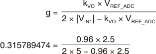
- A constant, g, is created to simplify resistor value computations.
- RA is now selected from the starting value of RB and the g constant.
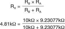
- RX can now be computed from the starting value of RB and the computed value for RA.


9.2.1.3 Application Curve
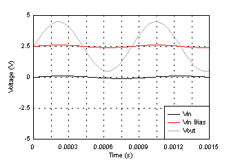 Figure 80. Voltage (V) vs Time (s)
9.2.2 Typical Application: General-Purpose Input Scaling
Figure 81 is an example application that demonstrates the flexibility of the PGA for general-purpose input scaling. VIN0 is a ±100-mV input that is ac-coupled into CH0. The PGA112 and PGA113 are powered from a 5-V supply voltage, VS, and configured with the VREF pin connected to VS/2 (2.5 V). VCH0 is the ±100-mV input, level-shifted and centered on VS/2 (2.5 V). A gain of 20 is applied to CH0, and because of the PGA113 configuration, the output voltage at VOUT is ±2 V centered on VS/2 (2.5 V).
CH1 is set to G = 1; through a resistive divider and scalar network, we can read ±5 V or 0 V. This setting provides bipolar to single-ended input scaling. Table 12 summarizes the scaling resistor values for RA, RX, and RB for different ADC Ref voltages. VREF_ADC is the reference voltage used for the ADC connected to the PGA112 and PGA113 output. It is assumed the ADC input range is 0 V to VREF_ADC. The Table 12 section gives the algorithm to compute resistor values for references not listed in Table 12. As a general guideline, RB should be chosen such that the input on-channel current multiplied by RB is less than or equal to the input offset voltage. This value ensures that the scaling network contributes no more error than the input offset voltage. Individual applications may require other design trade-offs.
 Figure 81. General-Purpose Input Scaling