SBOU231 October 2020 OPA3S328
2 EVM Circuit Description
The OPA3SS28 is a dual operational amplifier with integrated switches for transimpedance applications. This EVM provides access to the features and measure the performance of the OPA3S328. The OPA3S328EVM features two independent sites with OPA3S328 devices on different circuit configurations: site 1 and site 2.
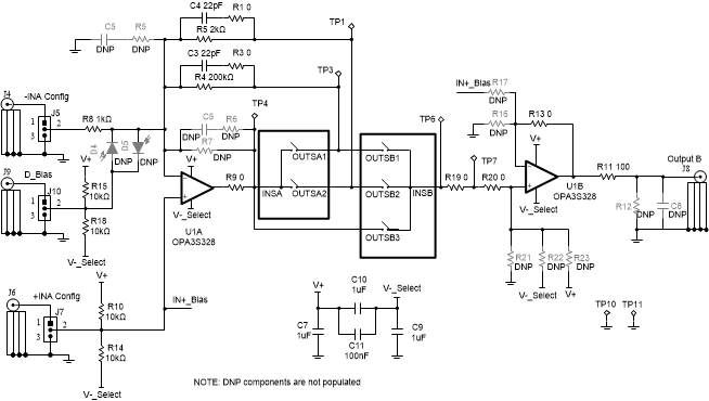
Site 1 incorporates OPA3S328 device U1 with amplifier U1A configured in the transimpedance configuration, with two possible transimpedance gains: 2 kΩ connected to switch SA1 and 200 kΩ connected to switch SA2. Amplifier U1B is configured by default as a high-impedance buffer, with switches SB1, SB2, and SB3 configured to sense the selected transimpedance gain. The simplified schematic of site 1 is displayed in Figure 2-1.
 Figure 2-1 OPA3S328EVM Site 1 Simplified Schematic
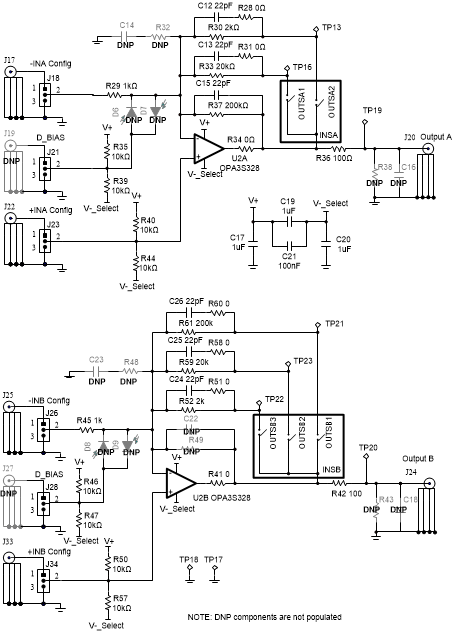
Site 2 incorporates OPA3S328 device U2 with amplifier U2A configured in the transimpedance configuration, with three possible transimpedance gains: 20 kΩ connected to switch SA1 , 2 kΩ to SA2 and a fixed feedback resistor and unswitched feedback resistor of 200 kΩ. Amplifier U2B is also configured in the transimpedance configuration, with three possible gains: 2 kΩ connected to switch SB3, 20 kΩ to switch SB2 and 200 kΩ to switch SB1.
The simplified schematic of site 2 is displayed in Figure 2-2.
 Figure 2-2 OPA3S328EVM Site 2 Simplified Schematic.