SBOU248 December 2020 TMCS1107 , TMCS1107-Q1
5.1 Schematics
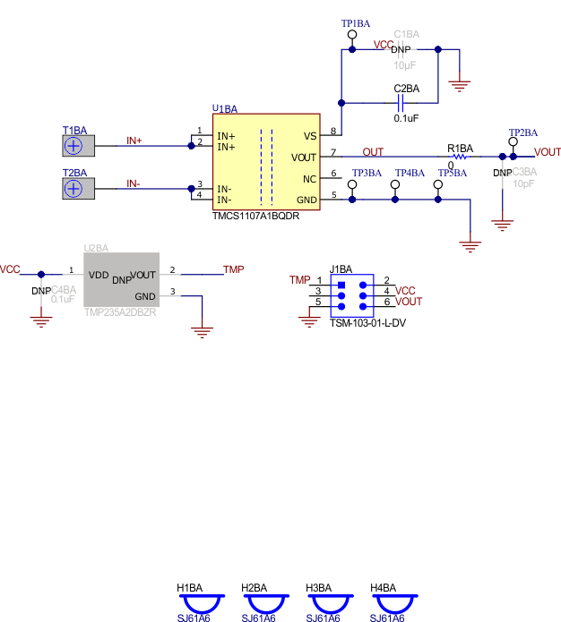
Figure 5-1 shows the schematic of the A1B sub board on the TMCS1107EVM PCB. Only the schematic for the bidirectional A1 (50 mV/A) gain variant is included as all variants use the same circuit and same PCB layout. All components associated with the 50-mV/A TMCS1107 A1 gain variant have the letter A appended at the end. The 100-mV/A A2 gain variant has B appended, the 200-mV/A A3 gain variant has C appended, and the 400-mV/A A4 gain variant has a D appended. All components labeled with a B after the number correspond to the bidirectional TMCS1107 devices, while all components labeled with a U after the number correspond to unidirectional TMCS1107 devices.
 Figure 5-1 Schematic for A1
Device