SBVA088 August 2022 TPS746-Q1
4.1 DRV Package
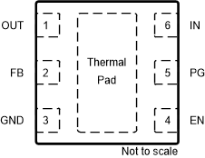
Figure 4-1 and Figure 4-2 show the TPS746-Q1 pin diagram (adjustable and fixed) for the DRV package. For a detailed description of the device pins, see the Pin Configuration and Functions section in the TPS746-Q1 data sheet.
 Figure 4-1 Pin Diagram
 (Adjustable TPS746-Q1 DRV Package)
Figure 4-2 Pin Diagram
(Fixed TPS746-Q1 DRV Package)
(Fixed TPS746-Q1 DRV Package)
Table 4-2 Pin FMA for Device Pins
Short-Circuited to Ground
| Pin Name | Pin No. | Description of Potential Failure Effect(s) | Failure Effect Class |
|---|---|---|---|
| OUT | 1 | The output voltage is near or at ground. The device enters current limit. The device may cycle in and out of thermal shutdown depending on power dissipation. | B |
| FB/NC | 2 | (Adjustable
output.) The device stops regulating. VOUT becomes equal
to VIN minus dropout because the pass transistor is
driven on as hard as possible. (Fixed output.) No effect. |
B, D |
| GND | 3 | — | D |
| EN | 4 | The device turns off. | B |
| PG | 5 | The PG function does not work. | D |
| IN | 6 | No output voltage. Input supply can be 0 V. | B |
Table 4-3 Pin FMA for Device Pins
Open-Circuited
| Pin Name | Pin No. | Description of Potential Failure Effect(s) | Failure Effect Class |
|---|---|---|---|
| OUT | 1 | Output voltage is disconnected from the load. | B |
| FB/NC | 2 | (Adjustable output.) Error amplifier input is left
floating, output voltage is not equal to set voltage. (Fixed output.) No effect. |
B, D |
| GND | 3 | The device may be disabled. | B |
| EN | 4 | The device may be disabled. | B |
| PG | 5 | The PG function does not work. | D |
| IN | 6 | No output voltage. | B |
Table 4-4 Pin FMA for Device Pins
Short-Circuited to Adjacent Pin
| Pin Name | Pin No. | Short to | Description of Potential Failure Effect(s) | Failure Effect Class |
|---|---|---|---|---|
| OUT | 1 | FB/NC (pin 2) | (Adjustable output.) VOUT is set to
VFB = 0.55 V. (Fixed output.) No effect. |
B, D |
| FB/NC | 2 | GND (pin 3) | (Adjustable output.) The device stops regulating.
VOUT becomes equal to VIN minus dropout
because the pass transistor is driven on as hard as possible. (Fixed output.) No effect. |
B, D |
| GND | 3 | EN (pin 4) | The output is forced off, VOUT is 0 V. | B |
| EN | 4 | PG (pin 5) | The device stays off. | B |
| PG | 5 | IN (pin 6) | The PG function does not work. | D |
Table 4-5 Pin FMA for Device Pins
Short-Circuited to
Supply
| Pin Name | Pin No. | Description of Potential Failure Effect(s) | Failure Effect Class |
|---|---|---|---|
| OUT | 1 | The output is not regulated. VOUT = VIN. | B |
| FB/NC | 2 | (Adjustable output.) The FB pin is damaged if
VIN is higher than 2 V. (Fixed output.) No effect. |
A, D |
| GND | 3 | No output voltage. Either input supply is at 0 V, or the input fuse is blown. | B |
| EN | 4 | The output is forced on regardless of the enable signal. | B |
| PG | 5 | The PG function does not work. | D |
| IN | 6 | No effect. | D |