SBVA088 August 2022 TPS746-Q1
1 Overview
This document contains information for the TPS746-Q1 (DRV and DRB packages) to aid in a functional safety system design. Information provided are:
- Functional safety failure in time (FIT) rates of the semiconductor component estimated by the application of industry reliability standards
- Component failure modes and their distribution (FMD) based on the primary function of the device
- Pin failure mode analysis (pin FMA)
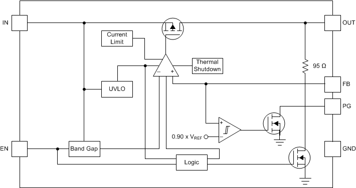
Figure 1-1 shows the adjustable version with open-drain, power-good functional block diagram for reference.
 Figure 1-1 Adjustable Version With
Open-Drain Power-Good
Figure 1-1 Adjustable Version With
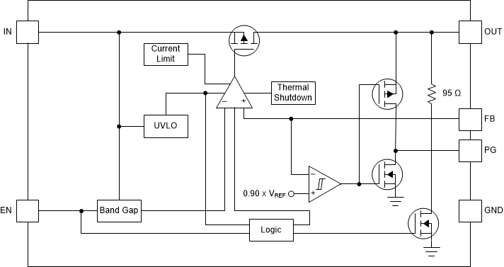
Open-Drain Power-GoodFigure 1-2 shows the adjustable version with push-pull, power-good functional block diagram for reference.
 Figure 1-2 Adjustable Version With
Push-Pull Power-Good
Figure 1-2 Adjustable Version With
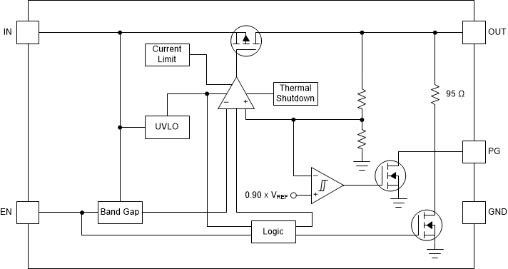
Push-Pull Power-GoodFigure 1-3 shows the fixed voltage version with open-drain, power-good functional block diagram for reference.
 Figure 1-3 Fixed Voltage Version With
Open-Drain Power-Good
Figure 1-3 Fixed Voltage Version With
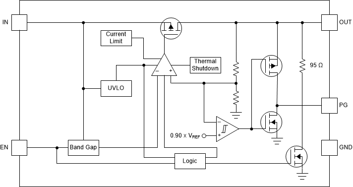
Open-Drain Power-GoodFigure 1-4 shows the fixed voltage version with push-pull, power-good functional block diagram for reference.
 Figure 1-4 Fixed Voltage Version With
Push-Pull Power-Good
Figure 1-4 Fixed Voltage Version With
Push-Pull Power-GoodThe TPS746-Q1 was developed using a quality-managed development process, but was not developed in accordance with the IEC 61508 or ISO 26262 standards.