SBVA093 December 2022 LP2992 , TPS786 , TPS7A30 , TPS7A3001-EP , TPS7A33 , TPS7A39 , TPS7A4501-SP , TPS7A47 , TPS7A47-Q1 , TPS7A4701-EP , TPS7A49 , TPS7A52 , TPS7A52-Q1 , TPS7A53 , TPS7A53-Q1 , TPS7A53A-Q1 , TPS7A53B , TPS7A54 , TPS7A54-Q1 , TPS7A57 , TPS7A7100 , TPS7A7200 , TPS7A7300 , TPS7A80 , TPS7A8300 , TPS7A83A , TPS7A84 , TPS7A84A , TPS7A85 , TPS7A85A , TPS7A87 , TPS7A89 , TPS7A90 , TPS7A91 , TPS7A92 , TPS7A94 , TPS7A96 , TPS7B7702-Q1 , TPS7H1111-SEP , TPS7H1111-SP , TPS7H1210-SEP
2 Comprehensive Review of Error in LDO's
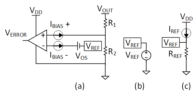
In a typical LDO, the voltage feedback amplifier (error amplifier) compares the sensed output voltage to the reference voltage and adjusts the feedback loop accordingly (Figure 2-1). The nonideal components of the error amplifier include the offset voltage (VOS) and bias currents (IBIAS). In an ideal LDO, there are no sources of error and the output voltage is configured using VREF, R1 and R2.

| (a) Basic structure including nonideal bias current and offset voltage of op-amps. (b) Reference voltage generated via a precision voltage. (c) Reference voltage generated via a precision current source and resistor. |
The output voltage error sources include the reference voltage, error amplifier, feedback resistors, and pass element. Other sources of error on the output voltage include load regulation and line regulation. An LDOs line and load regulation measure how the voltage reference, error amplifier and pass element react to changes in line voltage and load current, respectively.
The source of load regulation inside an LDO is concentrated around the error amplifier and pass element. The reference voltage is minimally affected, if at all, to changes in load current. In contrast, the reference voltage, the error amplifier and pass fet are all affected by changes in line, which combined make up the line regulation of an LDO. Thus, the reference voltage can be thought of as dependent on the line voltage, while the offset voltage can be thought of as dependent on both the line voltage and load current.
We can write an equation to describe the error, VE, on the output (Equation 2). The bias current flows into the resistor RFBx. If IBIAS+ is flowing into the error amplifier input, RFBx = R1 and the term IBIASRFBx is positive. If IBIAS+ is flowing out of the error amplifier input, RFBx = R2 and the term IBIASRFBx is negative.
A special use case exists such that the feedback resistors are removed and the feedback pin is directly tied to VOUT. In this case, Equation 2 can be modified to become Equation 3.