SBVS080J September 2006 – November 2016 TPS75100 , TPS75103 , TPS75105
PRODUCTION DATA.
- 1 Features
- 2 Applications
- 3 Description
- 4 Revision History
- 5 Pin Configuration and Functions
- 6 Specifications
- 7 Detailed Description
- 8 Application and Implementation
- 9 Power Supply Recommendations
- 10Layout
- 11Device and Documentation Support
- 12Mechanical, Packaging, and Orderable Information
7 Detailed Description
7.1 Overview
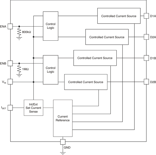
The TPS7510x linear low dropout (LDO) matching LED current source is optimized for low-power keypad and navigation pad LED backlighting applications. The device provides a constant current to up to four unmatched LEDs organized in two banks of two LEDs each in a common-cathode topology. Brightness can be varied from off to full brightness by inputting a pulse width modulation (PWM) signal on each enable pin (ENx, where x indicates LED bank A or B). Each bank has independent enable and brightness control, but current matching is done to all four channels concurrently. The input supply range is ideally suited for single-cell Li-Ion battery supplies and the TPS7510x can provide up to 25 mA per LED.
7.2 Functional Block Diagram

7.3 Feature Description
7.3.1 Load Regulation
The TPS7510x is designed to provide very tight load regulation. In the case of a fixed current source, the output load change is a change in voltage. Tight load regulation means that output voltages (LED forward voltages) with large variations can be used without impacting the fixed current being sourced by the output or the output-to-output current matching. The permissible variation on the output not only allows for large variations in white LED forward voltages, but even permits the use of different color LEDs on different outputs with minimal effect on output current.
7.3.2 Line Regulation
The TPS7510x is also designed to provide very tight line regulation. This architecture allows for voltage transient events to occur on the power supply (battery) without effecting the fixed output current levels or the output-to-output current matching. A prime example of such a supply transient event is the occurrence of a transmit pulse on the radio of a mobile handset. These transient pulses can cause variations of 300 mV and 600 mV on the supply to the TPS7510x. The line regulation limitation is that the lower supply voltage level of the event does not cause the input-to-output voltage difference to drop below the dropout voltage range.
7.4 Device Functional Modes
7.4.1 LED ON
Apply 1.2 V or more to ENx to turn the LED bank on.
7.4.2 LED OFF
Apply a voltage less than or equal to 0.4V to ENx to turn the LED bank off.