SBVS080J September   2006  – November 2016 TPS75100 , TPS75103 , TPS75105

PRODUCTION DATA.  

  1. Features
  2. Applications
  3. Description
  4. Revision History
  5. Pin Configuration and Functions
  6. Specifications
    1. 6.1 Absolute Maximum Ratings
    2. 6.2 ESD Ratings
    3. 6.3 Recommended Operating Conditions
    4. 6.4 Thermal Information
    5. 6.5 Electrical Characteristics
    6. 6.6 Typical Characteristics
  7. Detailed Description
    1. 7.1 Overview
    2. 7.2 Functional Block Diagram
    3. 7.3 Feature Description
      1. 7.3.1 Load Regulation
      2. 7.3.2 Line Regulation
    4. 7.4 Device Functional Modes
      1. 7.4.1 LED ON
      2. 7.4.2 LED OFF
  8. Application and Implementation
    1. 8.1 Application Information
      1. 8.1.1 Setting the Output Current Level
      2. 8.1.2 Limitations on LED Forward Voltages
      3. 8.1.3 Use of External Capacitors
      4. 8.1.4 Use of Unused Outputs or Tying Outputs Together
      5. 8.1.5 Use of Enable Pins for PWM Dimming
    2. 8.2 Typical Application
      1. 8.2.1 Design Requirements
      2. 8.2.2 Detailed Design Procedure
      3. 8.2.3 Application Curve
  9. Power Supply Recommendations
  10. 10Layout
    1. 10.1 Layout Guidelines
    2. 10.2 Layout Example
  11. 11Device and Documentation Support
    1. 11.1 Device Support
      1. 11.1.1 Development Support
      2. 11.1.2 Device Nomenclature
    2. 11.2 Documentation Support
      1. 11.2.1 Related Documentation
    3. 11.3 Related Links
    4. 11.4 Receiving Notification of Documentation Updates
    5. 11.5 Community Resources
    6. 11.6 Trademarks
    7. 11.7 Electrostatic Discharge Caution
    8. 11.8 Glossary
  12. 12Mechanical, Packaging, and Orderable Information

Layout

Layout Guidelines

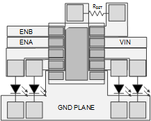
Figure 15 demonstrates an example layout for the WSON package.

Layout Example

TPS75100 TPS75103 TPS75105 pcb_layout_DSK_bvs080.gif Figure 15. Layout Example for the WSON (DSK) Package