SBVU077 October 2022
5 PCB Layout
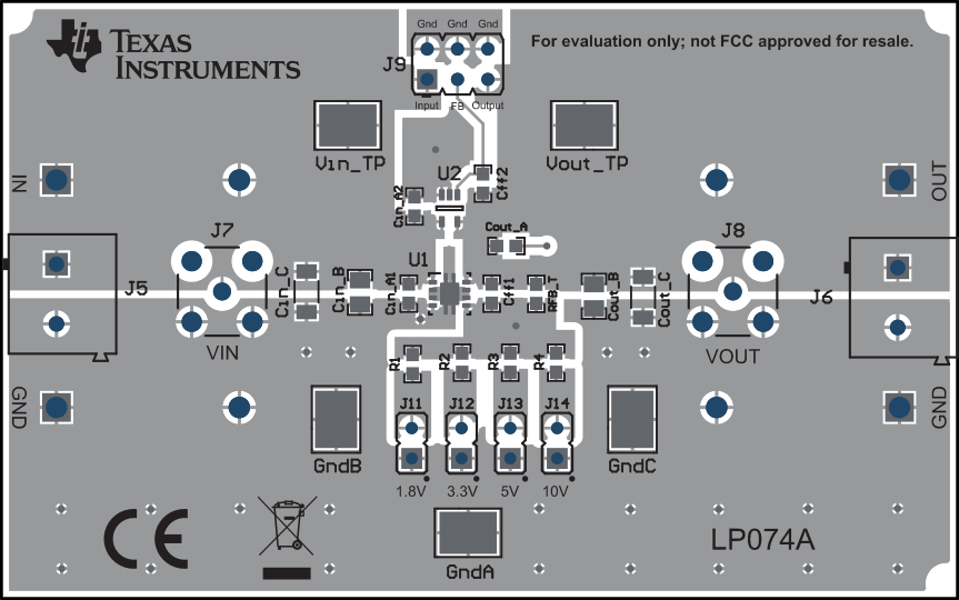
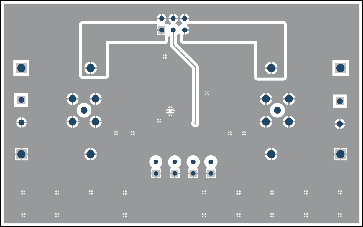
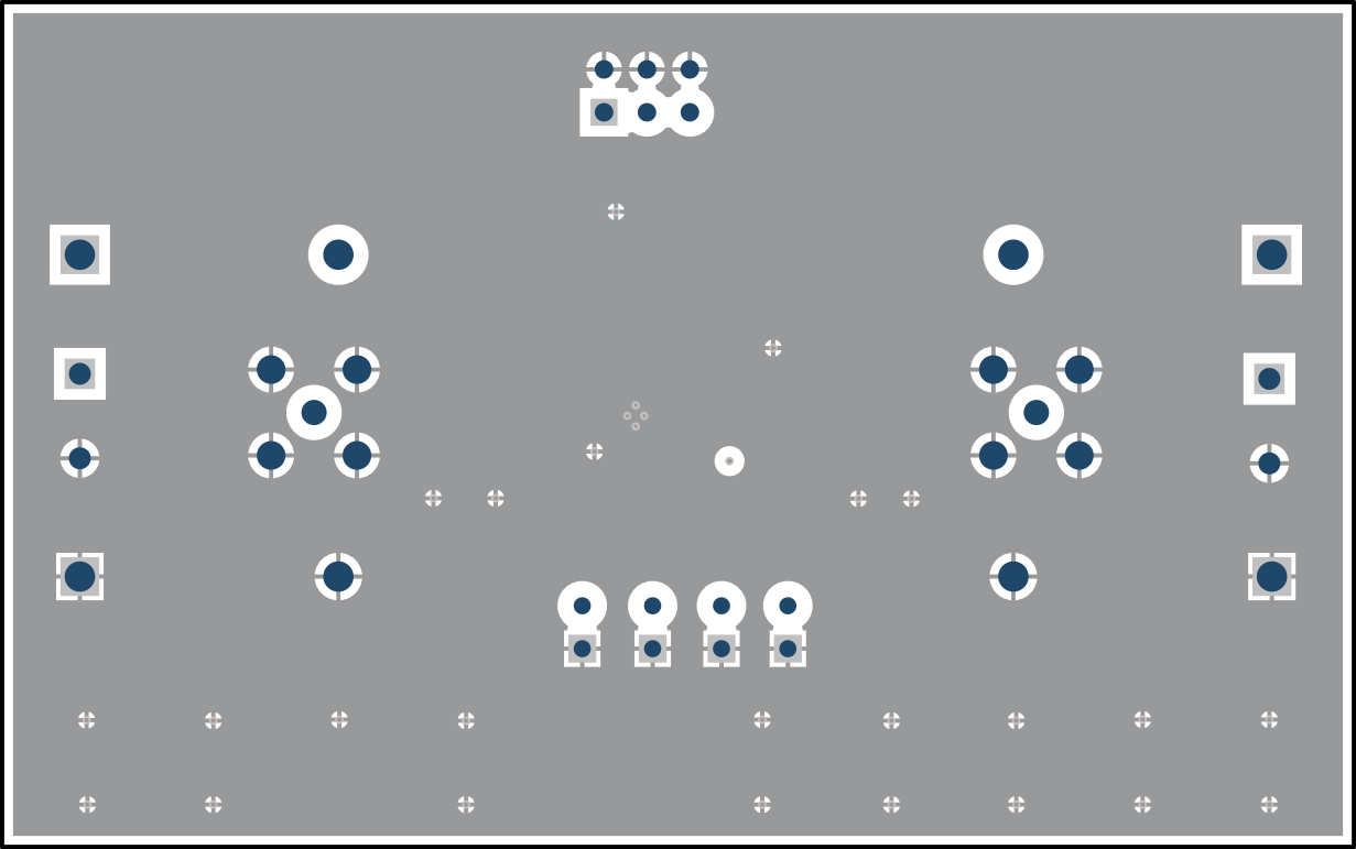
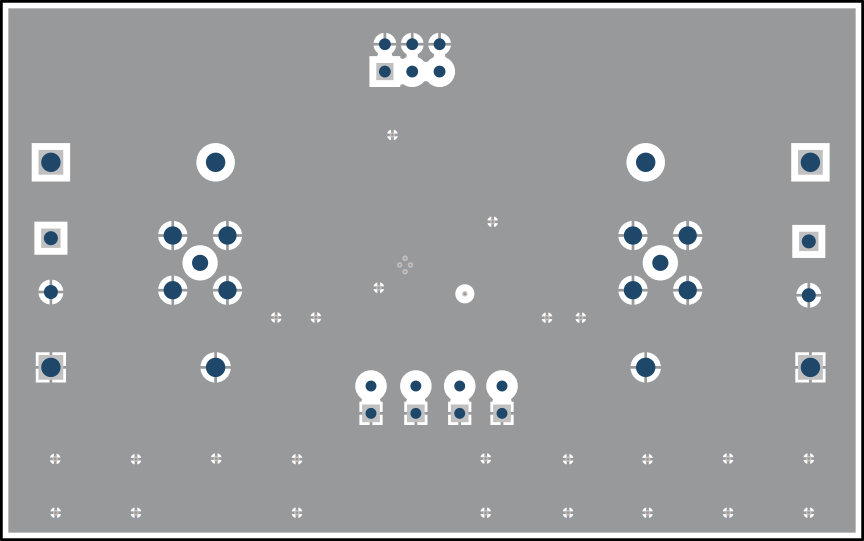
Figure 5-1 through Figure 5-4 depict the layout of the TPS715EVM-074.
 Figure 5-1 TPS715EVM-074 Top Layer
Routing
 Figure 5-3 TPS715EVM-074 Internal
Layer 2 Routing
 Figure 5-2 TPS715EVM-074 Internal
Layer 1 Routing
 Figure 5-4 TPS715EVM-074 Bottom Layer
Routing