SCAS862G November 2008 – July 2016 CDCE62005
PRODUCTION DATA.
- 1 Features
- 2 Applications
- 3 Description
- 4 Revision History
- 5 Pin Configuration and Functions
- 6 Specifications
- 7 Parameter Measurement Information
-
8 Detailed Description
- 8.1 Overview
- 8.2 Functional Block Diagrams
- 8.3
Feature Description
- 8.3.1 Phase Noise Analysis
- 8.3.2 Output To Output Isolation
- 8.3.3 Device Control
- 8.3.4 External Control Pins
- 8.3.5
Input Block
- 8.3.5.1 Universal Input Buffers (UIB)
- 8.3.5.2 LVDS Fail Safe Mode
- 8.3.5.3 Smart Multiplexer Controls
- 8.3.5.4 Smart Multiplexer Auto Mode
- 8.3.5.5 Smart Multiplexer Dividers
- 8.3.5.6 Output Block
- 8.3.5.7 Output Multiplexer Control
- 8.3.5.8 Output Buffer Control
- 8.3.5.9 Output Buffer Control - LVCMOS Configurations
- 8.3.5.10 Output Dividers
- 8.3.5.11 Digital Phase Adjust
- 8.3.5.12 Phase Adjust Example
- 8.3.5.13 Valid Register Settings for Digital Phase Adjust Blocks
- 8.3.5.14 Output Synchronization
- 8.3.5.15 Auxiliary Output
- 8.3.5.16 Synthesizer Block
- 8.3.5.17 Input Divider
- 8.3.5.18 Feedback and Feedback Bypass Divider
- 8.3.5.19 Internal Loop Filter Component Configuration
- 8.3.5.20 External Loop Filter Component Configuration
- 8.3.6 Digital Lock Detect
- 8.3.7 Crystal Input Interference
- 8.3.8 VCO Calibration
- 8.3.9 Startup Time Estimation
- 8.3.10 Analog Lock Detect
- 8.4 Device Functional Modes
- 8.5 Programming
- 8.6
Register Maps
- 8.6.1 Device Registers: Register 0 Address 0x00
- 8.6.2 Device Registers: Register 1 Address 0x01
- 8.6.3 Device Registers: Register 2 Address 0x02
- 8.6.4 Device Registers: Register 3 Address 0x03
- 8.6.5 Device Registers: Register 4 Address 0x04
- 8.6.6 Device Registers: Register 5 Address 0x05
- 8.6.7 Device Registers: Register 6 Address 0x06
- 8.6.8 Device Registers: Register 7 Address 0x07
- 8.6.9 Device Registers: Register 8 Address 0x08
- 9 Application and Implementation
- 10Power Supply Recommendations
- 11Layout
- 12Device and Documentation Support
- 13Mechanical, Packaging, and Orderable Information
11 Layout
11.1 Layout Guidelines
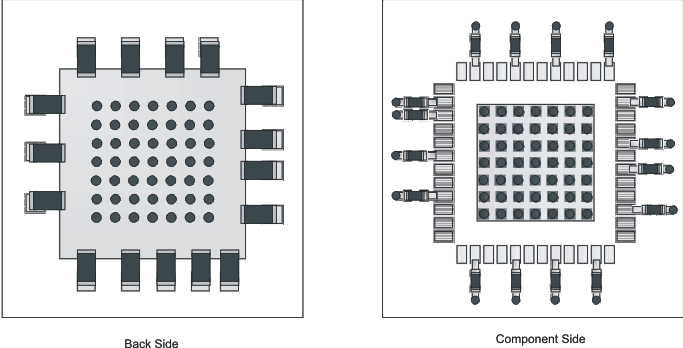
Figure 54 shows two conceptual layouts detailing recommended placement of power supply bypass capacitors. If the capacitors are mounted on the back side, 0402 components can be employed; however, soldering to the Thermal Dissipation Pad can be difficult. For component side mounting, use 0201 body size capacitors to facilitate signal routing. Keep the connections between the bypass capacitors and the power supply on the device as short as possible. Ground the other side of the capacitor using a low impedance connection to the ground plane.
11.2 Layout Example
 Figure 54. CDCE62005 Power Supply Bypassing