SCAS862G November 2008 – July 2016 CDCE62005
PRODUCTION DATA.
- 1 Features
- 2 Applications
- 3 Description
- 4 Revision History
- 5 Pin Configuration and Functions
- 6 Specifications
- 7 Parameter Measurement Information
-
8 Detailed Description
- 8.1 Overview
- 8.2 Functional Block Diagrams
- 8.3
Feature Description
- 8.3.1 Phase Noise Analysis
- 8.3.2 Output To Output Isolation
- 8.3.3 Device Control
- 8.3.4 External Control Pins
- 8.3.5
Input Block
- 8.3.5.1 Universal Input Buffers (UIB)
- 8.3.5.2 LVDS Fail Safe Mode
- 8.3.5.3 Smart Multiplexer Controls
- 8.3.5.4 Smart Multiplexer Auto Mode
- 8.3.5.5 Smart Multiplexer Dividers
- 8.3.5.6 Output Block
- 8.3.5.7 Output Multiplexer Control
- 8.3.5.8 Output Buffer Control
- 8.3.5.9 Output Buffer Control - LVCMOS Configurations
- 8.3.5.10 Output Dividers
- 8.3.5.11 Digital Phase Adjust
- 8.3.5.12 Phase Adjust Example
- 8.3.5.13 Valid Register Settings for Digital Phase Adjust Blocks
- 8.3.5.14 Output Synchronization
- 8.3.5.15 Auxiliary Output
- 8.3.5.16 Synthesizer Block
- 8.3.5.17 Input Divider
- 8.3.5.18 Feedback and Feedback Bypass Divider
- 8.3.5.19 Internal Loop Filter Component Configuration
- 8.3.5.20 External Loop Filter Component Configuration
- 8.3.6 Digital Lock Detect
- 8.3.7 Crystal Input Interference
- 8.3.8 VCO Calibration
- 8.3.9 Startup Time Estimation
- 8.3.10 Analog Lock Detect
- 8.4 Device Functional Modes
- 8.5 Programming
- 8.6
Register Maps
- 8.6.1 Device Registers: Register 0 Address 0x00
- 8.6.2 Device Registers: Register 1 Address 0x01
- 8.6.3 Device Registers: Register 2 Address 0x02
- 8.6.4 Device Registers: Register 3 Address 0x03
- 8.6.5 Device Registers: Register 4 Address 0x04
- 8.6.6 Device Registers: Register 5 Address 0x05
- 8.6.7 Device Registers: Register 6 Address 0x06
- 8.6.8 Device Registers: Register 7 Address 0x07
- 8.6.9 Device Registers: Register 8 Address 0x08
- 9 Application and Implementation
- 10Power Supply Recommendations
- 11Layout
- 12Device and Documentation Support
- 13Mechanical, Packaging, and Orderable Information
6 Specifications
6.1 Absolute Maximum Ratings
over operating free-air temperature range (unless otherwise noted)(1)| MIN | MAX | UNIT | ||
|---|---|---|---|---|
| VCC | Supply voltage range(2) | –0.5 | 4.6 | V |
| VI | Input voltage range(3) | –0.5 | VCC + 0.5 | V |
| VO | Output voltage range(3) | –0.5 | VCC + 0.5 | V |
| Input Current (VI < 0, VI > VCC) | ±20 | mA | ||
| Output current for LVPECL/LVCMOS Outputs (0 < VO < VCC) | ±50 | mA | ||
| TJ | Junction temperature | 125 | °C | |
| Tstg | Storage temperature | –65 | 150 | °C |
(1) Stresses beyond those listed under absolute maximum ratings may cause permanent damage to the device. These are stress ratings only and functional operation of the device at these or any other conditions beyond those indicated under recommended operating conditions is not implied. Exposure to absolute–maximum–rated conditions for extended periods may affect device reliability.
(2) All supply voltages have to be supplied simultaneously.
(3) The input and output negative voltage ratings may be exceeded if the input and output clamp–current ratings are observed.
6.2 ESD Ratings
| MIN | MAX | UNIT | |||
|---|---|---|---|---|---|
| V(ESD) | Electrostatic discharge | Human body model (HBM), per ANSI/ESDA/JEDEC JS-001, all pins(1) | 2000 | V | |
| Charged device model (CDM), per JEDEC specification JESD22-C101, all pins(2) | 750 | ||||
(1) JEDEC document JEP155 states that 500-V HBM allows safe manufacturing with a standard ESD control process.
(2) JEDEC document JEP157 states that 250-V CDM allows safe manufacturing with a standard ESD control process.
6.3 Thermal Information(2)(3)
| THERMAL METRIC(1) | RGZ | UNIT | |
|---|---|---|---|
| 48 PINS | |||
| RθJA | Junction-to-ambient thermal resistance | 28.9(5) | °C/W |
| 20.4(6) | |||
| 27.3(7) | |||
| 20.3(8) | |||
| RθJC(top) | Junction-to-case (top) thermal resistance | 12.9 | °C/W |
| RθJB | Junction-to-board thermal resistance | 4.0 | °C/W |
| ψJT | Junction-to-top characterization parameter | 0.2 | °C/W |
| ψJB | Junction-to-board characterization parameter | 4.0 | °C/W |
| RθJC(bot) | Junction-to-case (bottom) thermal resistance | 0.9 | °C/W |
| θJP | Junction-to-pad(4) | 2(5) | °C/W |
| 2(6) | |||
| 2(7) | |||
| 2(8) | |||
(1) For more information about traditional and new thermal metrics, see the Semiconductor and IC Package Thermal Metrics application report, SPRA953.
(2) The package thermal impedance is calculated in accordance with JESD 51 and JEDEC2S2P (high-k board).
(3) Connected to GND with 36 thermal vias (0,3 mm diameter).
(4) θJP (Junction – Pad) is used for the QFN Package, because the main heat flow is from the Junction to the GND-Pad of the QFN.
(5) JEDEC Compliant Board (6X6 VIAs on PAD), Ariflow = 0 LFM
(6) JEDEC Compliant Board (6X6 VIAs on PAD) , Airflow = 100 LFM
(7) Recommended Layout (7X7 VIAs on PAD), Airflow = 0 LFM
(8) Recommended Layout (7X7 VIAs on PAD), Airflow = 100 LFM
6.4 Electrical Characteristics
recommended operating conditions for the CDCE62005 device for under the specified Industrial temperature range of –40°C to 85°C| PARAMETER | TEST CONDITIONS | MIN | TYP(1) | MAX | UNIT | |||
|---|---|---|---|---|---|---|---|---|
| POWER SUPPLY | ||||||||
| VCC | Supply voltage | 3 | 3.3 | 3.6 | V | |||
| VCC_PLL, VCC_IN, VCC_VCO, VCCA | Analog supply voltage | 3 | 3.3 | 3.6 | ||||
| PLVPECL | REF at 30.72,MHz, Outputs are LVPECL | Output 1 = 491.52 MHz Output 2 = 245.76 MHz Output 3 = 122.88 MHz Output 4 = 61.44 MHz Output 5 = 30.72 MHz In case of LVCMOS Output1 = 245.76 MHz |
1.9 | W | ||||
| PLVDS | REF at 30.72 MHz, Outputs are LVDS | 1.65 | W | |||||
| PLVCMOS | REF at 30.72 MHz, Outputs are LVCMOS | 1.8 | W | |||||
| POFF | REF at 30.72 MHz | Dividers are disabled. Outputs are disabled. | 0.75 | W | ||||
| PPD | Device is powered down | 20 | mW | |||||
| DIFFERENTIAL INPUT MODE (PRI_REF, SEC_REF) | ||||||||
| VIN | Differential input amplitude (VIN – V/IN) | 0.1 | 1.3 | V | ||||
| VIC | Common-mode input voltage | 1.0 | VCC–0.3 | V | ||||
| IIH | Differential input current high (no internal termination) | VI = VCC, VCC = 3.6 V | 20 | μA | ||||
| IIL | Differential input current low (no internal termination) | VI = 0 V, VCC = 3.6 V | –20 | 20 | μA | |||
| Input Capacitance on PRI_REF, SEC_REF | 3 | pF | ||||||
| CRYSTAL INPUT SPECIFICATIONS | ||||||||
| On-chip load capacitance | 10 | pF | ||||||
| Equivalent series resistance (ESR) | 50 | Ω | ||||||
| LVCMOS INPUT MODE (SPI_CLK, SPI_MOSI, SPI_LE, Power_Down, SYNC, REF_SEL, PRI_REF, SEC_REF ) | ||||||||
| Low-level input voltage LVCMOS, | 0 | 0.3 x VCC | V | |||||
| High-level input voltage LVCMOS | 0.7 x VCC | VCC | V | |||||
| VIK | LVCMOS input clamp voltage | VCC = 3 V, II = –18 mA | –1.2 | V | ||||
| IIH | LVCMOS input current | VI = VCC, VCC = 3.6 V | 20 | μA | ||||
| IIL | LVCMOS input (Except PRI_REF and SEC_REF) | VI = 0 V, VCC = 3.6 V | –10 | –40 | μA | |||
| IIL | LVCMOS input (PRI_REF and SEC_REF) | VI = 0 V, VCC = 3.6 V | –10 | 10 | μA | |||
| CI | Input capacitance | VI = 0 V or VCC | 3 | pF | ||||
| SPI OUTPUT (MISO) / PLL_LOCK OUTPUT | ||||||||
| IOH | High-level output current | VCC = 3.3 V, | VO = 1.65 V | –30 | mA | |||
| IOL | Low-level output current | VCC = 3.3 V, | VO = 1.65 V | 33 | mA | |||
| VOH | High-level output voltage for LVCMOS outputs | VCC = 3 V, | IOH = −100 μA | VCC–0.5 | V | |||
| VOL | Low-level output voltage for LVCMOS outputs | VCC = 3 V, | IOL = 100 μA | 0.3 | V | |||
| CO | Output capacitance on MISO | VCC = 3.3 V; VO = 0 V or VCC(1) | 3 | pF | ||||
| IOZH | 3-state output current | VO = VCC
VO = 0 V |
5 | μA | ||||
| IOZL | –5 | |||||||
| EEPROM | ||||||||
| EEcy | Programming cycle of EEPROM | 100 | 1000 | Cycles | ||||
| EEret | Data retention | 10 | Years | |||||
| VBB | ||||||||
| VBB | Termination voltage for reference inputs. | IBB = –0.2 mA, Depending on the setting. | 0.9 | 1.9 | V | |||
| INPUT BUFFERS INTERNAL TERMINATION RESISTORS (PRI_REF and SEC_REF) | ||||||||
| Termination resistance | Single ended | 50 | Ω | |||||
| PHASE DETECTOR | ||||||||
| fCPmax | Charge pump frequency | 0.04 | 40 | MHz | ||||
| LVCMOS OUTPUT / AUXILIARY OUTPUT(1) | ||||||||
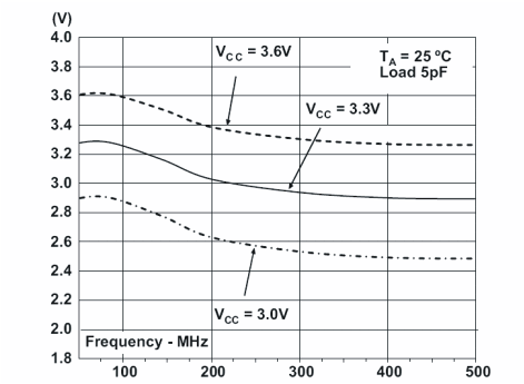
| fclk | Output frequency (see Figure 7) | Load = 5 pF to GND | 0 | 250 | MHz | |||
| VOH | High-level output voltage for LVCMOS outputs | VCC = min to max | IOH = –100 μA | VCC –0.5 | ||||
| VOL | Low-level output voltage for LVCMOS outputs | VCC = min to max | IOL =100 µA | 0.3 | V | |||
| IOH | High-level output current | VCC = 3.3 V | VO = 1.65 V | –30 | mA | |||
| IOL | Low-level output current | VCC = 3.3 V | VO = 1.65 V | 33 | mA | |||
| tpho | Reference (PRI_REF or SEC_REF) to Output Phase offset | Outputs are set to 122.88 MHz, Reference at 30.72 MHz | 0.35 | ns | ||||
| tpd(LH)/
tpd(HL) |
Propagation delay from PRI_REF or SEC_REF to Outputs | Crosspoint to VCC/2, Bypass Mode | 4 | ns | ||||
| tsk(o) | Skew, output to output For Y0 to Y4 | All Outputs set at 200 MHz, Reference = 200 MHz | 75 | ps | ||||
| CO | Output capacitance on Y0 to Y4 | VCC = 3.3 V; VO = 0 V or VCC | 5 | pF | ||||
| IOZH | 3-State LVCMOS output current | VO = VCC | 5 | μA | ||||
| IOZL | VO = 0 V | –5 | μA | |||||
| IOPDH | Power Down output current | VO = VCC | 25 | μA | ||||
| IOPDL | VO = 0 V | 5 | μA | |||||
| Duty cycle LVCMOS | 45% | 55% | ||||||
| tslew-rate | Output rise/fall slew rate | 3.6 | 5.2 | V/ns | ||||
| LVDS OUTPUT(1)(3) | ||||||||
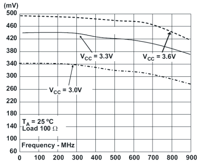
| fclk | Output frequency (see Figure 8) | Configuration Load | 0 | 800 | MHz | |||
| |VOD| | Differential output voltage | RL = 100 Ω | 270 | 550 | mV | |||
| ΔVOD | LVDS VOD magnitude change | 50 | mV | |||||
| Offset Voltage | 40°C to 85°C | 1.24 | V | |||||
| ΔVOS | VOS magnitude change | 40 | mV | |||||
| Short circuit Vout+ to ground | VOUT = 0 | 27 | mA | |||||
| Short circuit Vout– to ground | VOUT = 0 | 27 | mA | |||||
| tpho | Reference (PRI_REF or SEC_REF) to output phase offset | Outputs are set to 491.52 MHz Reference at 30.72 MHz |
1.65 | ns | ||||
| tpd(LH)/tpd(HL) | Propagation delay from PRI_REF or SEC_REF to outputs | Crosspoint to Crosspoint, Bypass Mode | 3.1 | ns | ||||
| tsk(o)(2) | Skew, output to output For Y0 to Y4 | All Outputs set at 200 MHz | 25 | ps | ||||
| CO | Output capacitance on Y0 to Y4 | VCC = 3.3 V; VO = 0 V or VCC | 5 | pF | ||||
| IOPDH | Power down output current | VO = VCC | 25 | μA | ||||
| IOPDL | Power down output current | VO = 0 V | 5 | μA | ||||
| Duty cycle | 45% | 55% | ||||||
| tr / tf | Rise and fall time | 20% to 80% of VOUT(PP) | 110 | 160 | 190 | ps | ||
| LVCMOS-TO-LVDS(4) | ||||||||
| tskP_c | Output skew between LVCMOS and LVDS outputs | VCC/2 to Crosspoint. Output are at the same output frequency and use the same output divider configuration. | 0.9 | 1.4 | 1.9 | ns | ||
| LVPECL OUTPUT | ||||||||
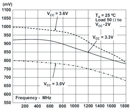
| fclk | Output frequency, Configuration load (see Figure 9 and Figure 10) | 0 | 1500 | MHz | ||||
| VOH | LVPECL high-level output voltage load | VCC –1.06 | VCC –0.88 | V | ||||
| VOL | LVPECL low-level output voltage load | VCC–2.02 | VCC–1.58 | V | ||||
| |VOD| | Differential output voltage | 610 | 970 | mV | ||||
| tpho | Reference to Output Phase offset | Outputs are set to 491.52 MHz, Reference at 30.72 MHz | 1.47 | ns | ||||
| tpd(LH)/ tpd(HL) |
Propagation delay from PRI_REF or SEC_REF to outputs | Crosspoint to Crosspoint, Bypass Mode | 3.4 | ns | ||||
| tsk(o) | Skew, output to output For Y0 to Y4 | All Outputs set at 200 MHz | 25 | ps | ||||
| CO | Output capacitance on Y0 to Y4 | VCC = 3.3 V; VO = 0 V or VCC | 5 | pF | ||||
| IOPDH | Power Down output current | VO = VCC | 25 | μA | ||||
| IOPDL | VO = 0 V | 5 | μA | |||||
| Duty Cycle | 45% | 55% | ||||||
| tr / tf | Rise and fall time | 20% to 80% of VOUT(PP) | 55 | 75 | 135 | ps | ||
| LVDS-TO-LVPECL | ||||||||
| tskP_C | Output skew between LVDS and LVPECL outputs | Crosspoint to Crosspoint output dividers are configured identically. | 0.9 | 1.1 | 1.3 | ns | ||
| LVCMOS-TO-LVPECL | ||||||||
| tskP_C | Output skew between LVCMOS and LVPECL outputs | VCC/2 to Crosspoint output dividers are configured identically. | –150 | 260 | 700 | ps | ||
| LVPECL HI-SWING OUTPUT | ||||||||
| VOH | LVPECL high-level output voltage load | VCC –1.11 | VCC –0.87 | V | ||||
| VOL | LVPECL low-level output voltage load | VCC –2.06 | VCC –1.73 | V | ||||
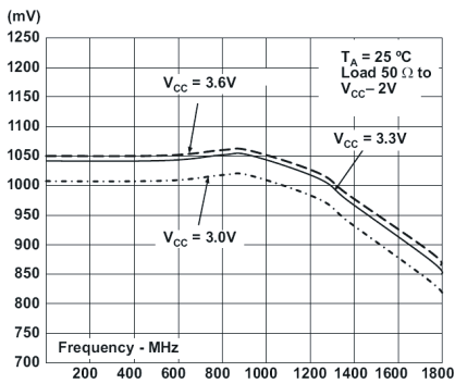
| |VOD| | Differential output voltage | 760 | 1160 | mV | ||||
| tr / tf | Rise and fall time | 20% to 80% of VOUT(PP) | 55 | 75 | 135 | ps | ||
(1) All typical values are at VCC = 3.3 V, temperature = 25°C
(2) The tsk(o) specification is only valid for equal loading of all outputs.
(3) The phase of LVCMOS is lagging in reference to the phase of LVDS.
(4) All typical values are at VCC = 3.3 V, temperature = 25°C
6.5 Timing Requirements
over recommended ranges of supply voltage, load and operating free air temperature (unless otherwise noted)6.6 SPI Bus Timing Characteristics
| MIN | NOM | MAX | UNIT | |||
|---|---|---|---|---|---|---|
| fClock | Clock Frequency for the SPI_CLK | 20 | MHz | |||
| t1 | SPI_LE to SPI_CLK setup time | See Figure 1 and Figure 2 | 10 | ns | ||
| t2 | SPI_MOSI to SPI_CLK setup time | See Figure 1 and Figure 2 | 10 | ns | ||
| t3 | SPI_MOSI to SPI_CLK hold time | See Figure 1 and Figure 2 | 10 | ns | ||
| t4 | SPI_CLK high duration | See Figure 1 and Figure 2 | 25 | ns | ||
| t5 | SPI_CLK low duration | See Figure 1 and Figure 2 | 25 | ns | ||
| t6 | SPI_CLK to SPI_LE Hold time | See Figure 1 and Figure 2 | 10 | ns | ||
| t7 | SPI_LE Pulse Width | See Figure 1 and Figure 2 | 20 | ns | ||
| t8 | SPI_CLK to MISO data valid | See Figure 2 | 10 | ns | ||
| t9 | SPI_LE to SPI_MISO Data Valid | See Figure 2 | 10 | ns | ||
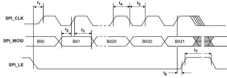 Figure 1. Timing Diagram for SPI Write Command
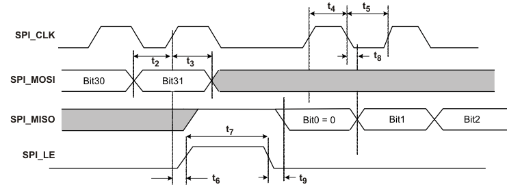 Figure 2. Timing Diagram for SPI Read Command
6.7 Typical Characteristics
