SCDU040 November 2024 TMUX7308F , TMUX7309F , TMUX7348F , TMUX7349F
2.2 Setup
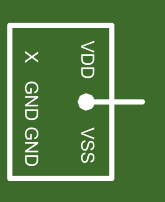
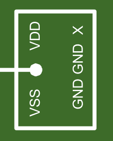
- All 16 generic signal pathway headers contain six pins. Figure 2-1 and Figure 2-2 show the generalized pinout of the headers for the left and right sides of the board respectively. Note that the orientation is based on J1 being on the top of the board.
 Figure 2-1 Left Side Jumper (J4-J11) Configuration or Pinout
 Figure 2-2 Right Side Jumper (J12,13,J16-J21) Configuration or Pinout