SCPS202C October 2009 – May 2016 TCA9539
PRODUCTION DATA.
- 1 Features
- 2 Applications
- 3 Description
- 4 Revision History
- 5 Pin Configuration and Functions
- 6 Specifications
- 7 Parameter Measurement Information
- 8 Detailed Description
- 9 Application and Implementation
- 10Power Supply Recommendations
- 11Layout
- 12Device and Documentation Support
- 13Mechanical, Packaging, and Orderable Information
8 Detailed Description
8.1 Overview
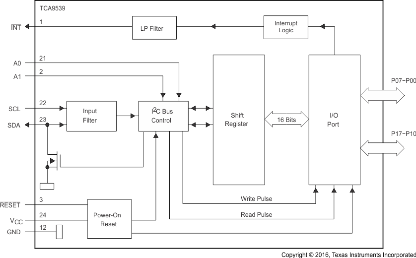
The TCA9539 is a 16-bit Input-Output expander for the two-line bidirectional bus (I2C) designed for 1.65-V to 5.5-V VCC operation. It provides general-purpose remote I/O expansion for most microcontroller families via the I2C interface ,serial clock (SCL) and serial data (SDA).
The TCA9539 consists of two 8-bit Configuration (input or output selection), Input Port, Output Port, and Polarity Inversion (active-high or active-low operation) registers. At power-on, the I/Os are configured as inputs. The system master can enable the I/Os as either inputs or outputs by writing to the I/O configuration register bits. The data for each input or output is kept in the corresponding Input or output register. The polarity of the Input Port register can be inverted with the Polarity Inversion register. All registers can be read by the system master.
The system master can reset the TCA9539 in the event of a time-out or other improper operation by asserting a low in the RESET input. The power-on reset puts the registers in their default state and initializes the I2C-SMBus state machine. Asserting RESET causes the same reset-initialization to occur without depowering the part.
The TCA9539 open-drain interrupt (INT) output is activated when any input state differs from its corresponding Input Port register state and is used to indicate to the system master that an input state has changed.
INT can be connected to the interrupt input of a microcontroller. By sending an interrupt signal on this line, the remote I/O can inform the microcontroller if there is incoming data on its ports without having to communicate via the I2C bus. Thus, the TCA9539 can remain a simple slave device.
The device outputs (latched) have high-current drive capability for directly driving LEDs. The device has low current consumption.
The TCA9539 is similar to the PCA9555, except for the removal of the internal I/O pull-up resistor, which greatly reduces power consumption when the I/Os are held low, replacement of A2 with RESET, and a different address range. The TCA9539 is equivalent to the PCA9539 with lower voltage support (down to VCC = 1.65 V), and also improved power-on-reset circuitry for different application scenarios.
Two hardware pins (A0 and A1) are used to program and vary the fixed I2C address and allow up to four devices to share the same I2C bus or SMBus.
8.2 Functional Block Diagram
8.3 Feature Description
8.3.1 I/O Port
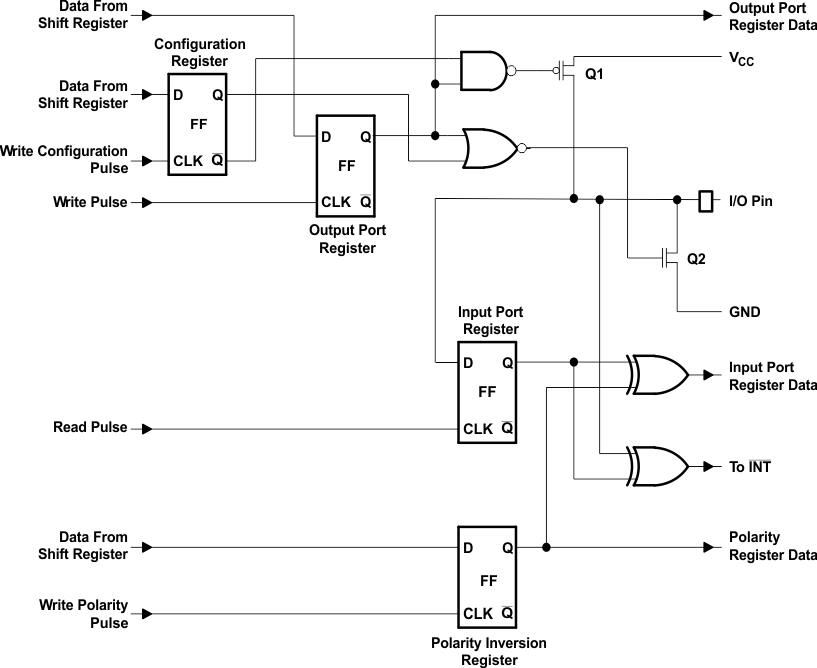
When an I/O is configured as an input, FETs Q1 and Q2 are off, which creates a high-impedance input. The input voltage may be raised above VCC to a maximum of 5.5 V.
If the I/O is configured as an output, Q1 or Q2 is enabled, depending on the state of the Output Port register. In this case, there are low-impedance paths between the I/O pin and either VCC or GND. The external voltage applied to this I/O pin must not exceed the recommended levels for proper operation.
8.3.2 RESET Input
A reset can be accomplished by holding the RESET pin low for a minimum of tW. The TCA9539 registers and I2C/SMBus state machine are held in their default states until RESET is once again high. This input requires a pull-up resistor to VCC, if no active connection is used.
8.3.3 Interrupt (INT) Output
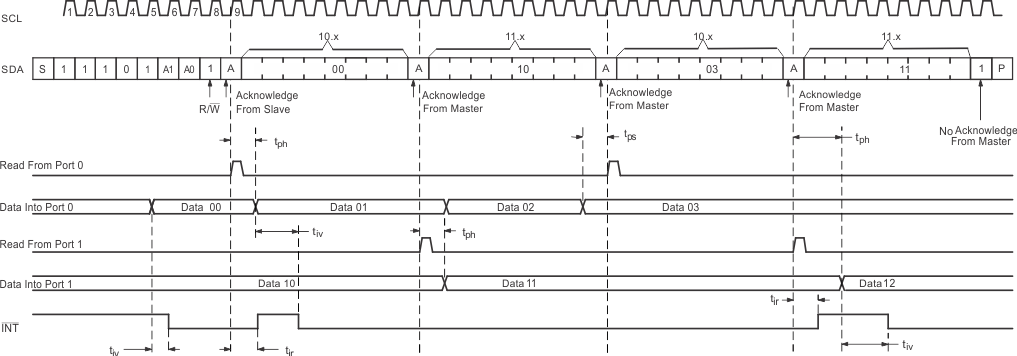
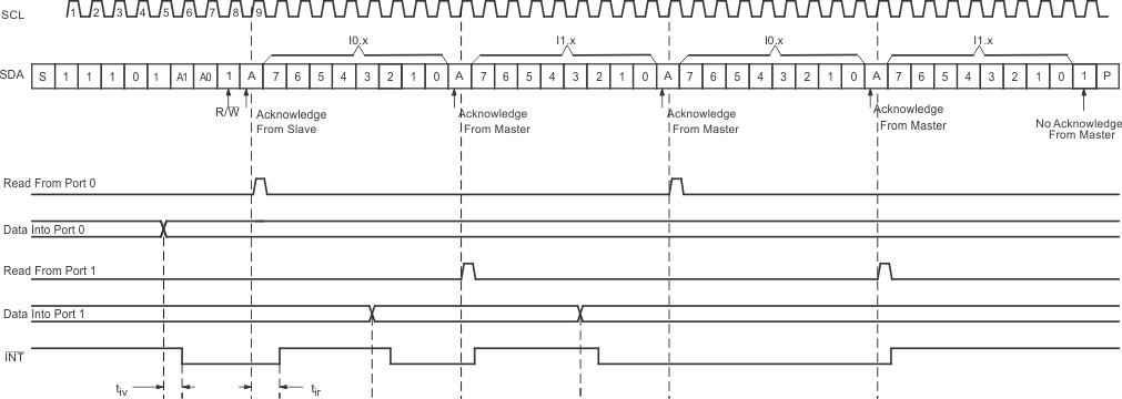
An interrupt is generated by any rising or falling edge of the port inputs in the input mode. After time tiv, the signal INT is valid. Resetting the interrupt circuit is achieved when data on the port is changed to the original setting or data is read from the port that generated the interrupt. Resetting occurs in the read mode at the acknowledge (ACK) bit after the rising edge of the SCL signal. Note that the INT is reset at the ACK just before the byte of changed data is sent. Interrupts that occur during the ACK clock pulse can be lost (or be very short) because of the resetting of the interrupt during this pulse. Each change of the I/Os after resetting is detected and is transmitted as INT.
Reading from or writing to another device does not affect the interrupt circuit, and a pin configured as an output cannot cause an interrupt. Changing an I/O from an output to an input may cause a false interrupt to occur if the state of the pin does not match the contents of the Input Port register. Because each 8-bit port is read independently, the interrupt caused by port 0 is not cleared by a read of port 1, or vice versa.
INT has an open-drain structure and requires a pull-up resistor to VCC.
8.4 Device Functional Modes
8.4.1 Power-On Reset
When power (from 0 V) is applied to VCC, an internal power-on reset holds the TCA9539 in a reset condition until VCC has reached VPOR R. At that point, the reset condition is released and the TCA9539 registers and I2C-SMBus state machine initialize to their default states. After that, VCC must be lowered to below VPORF and then back up to the operating voltage for a power-reset cycle.
8.5 Programming
8.5.1 I2C Interface
The TCA9539 has a standard bidirectional I2C interface that is controlled by a master device in order to be configured or read the status of this device. Each slave on the I2C bus has a specific device address to differentiate between other slave devices that are on the same I2C bus. Many slave devices require configuration upon startup to set the behavior of the device. This is typically done when the master accesses internal register maps of the slave, which have unique register addresses. A device can have one or multiple registers where data is stored, written, or read. For more information see Understanding the I2C Bus, SLVA704.
The physical I2C interface consists of the serial clock (SCL) and serial data (SDA) lines. Both SDA and SCL lines must be connected to VCC through a pull-up resistor. The size of the pull-up resistor is determined by the amount of capacitance on the I2C lines. For further details, see I2C Pull-up Resistor Calculation, SLVA689. Data transfer may be initiated only when the bus is idle. A bus is considered idle if both SDA and SCL lines are high after a STOP condition. See Table 1.
Figure 25 and Figure 26 show the general procedure for a master to access a slave device:
- If a master wants to send data to a slave:
- Master-transmitter sends a START condition and addresses the slave-receiver.
- Master-transmitter sends data to slave-receiver.
- Master-transmitter terminates the transfer with a STOP condition.
- If a master wants to receive or read data from a slave:
- Master-receiver sends a START condition and addresses the slave-transmitter.
- Master-receiver sends the requested register to read to slave-transmitter.
- Master-receiver receives data from the slave-transmitter.
- Master-receiver terminates the transfer with a STOP condition.
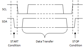 Figure 25. Definition of Start and Stop Conditions
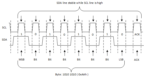 Figure 26. Bit Transfer
Table 1 shows the interface definition.
Table 1. Interface Definition
| BYTE | BIT | |||||||
| 7 (MSB) | 6 | 5 | 4 | 3 | 2 | 1 | 0 (LSB) | |
| I2C slave address | H | H | H | L | H | A1 | A0 | R/W |
| P0x I/O data bus | P07 | P06 | P05 | P04 | P03 | P02 | P01 | P00 |
| P1x I/O data bus | P17 | P16 | P15 | P14 | P13 | P12 | P11 | P10 |
8.6 Register Maps
8.6.1 Device Address
Figure 27 shows the address byte of the TCA9539.
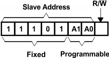 Figure 27. TCA9539 Address
Table 2 shows the address reference of the TCA9539.
Table 2. Address Reference
| INPUTS | I2C BUS SLAVE ADDRESS | |
|---|---|---|
| A1 | A0 | |
| L | L | 116 (decimal), 0x74 (hexadecimal) |
| L | H | 117 (decimal), 0x75 (hexadecimal) |
| H | L | 118 (decimal), 0x76 (hexadecimal) |
| H | H | 119 (decimal), 0x77 (hexadecimal) |
The last bit of the slave address defines the operation (read or write) to be performed. A high (1) selects a read operation, while a low (0) selects a write operation.
Note that the I2C addresses shown above are the 7-bit, right-justified hexadecimal values.
8.6.2 Control Register and Command Byte
Following the successful acknowledgment of the address byte, the bus master sends a command byte shown in Table 3 that is stored in the control register in the TCA9539. Three bits of this data byte state the operation (read or write) and the internal register (input, output, Polarity Inversion or Configuration) that is affected. This register can be written or read through the I2C bus. The command byte is sent only during a write transmission.
When a command byte has been sent, the register pair that was addressed continues to be accessed by reads until a new command byte has been sent. Figure 28 shows the control register bits.
 Figure 28. Control Register Bits
Table 3. Command Byte
| CONTROL REGISTER BITS | COMMAND BYTE (HEX) |
REGISTER | PROTOCOL | POWER-UP DEFAULT |
||
|---|---|---|---|---|---|---|
| B2 | B1 | B0 | ||||
| 0 | 0 | 0 | 0x00 | Input Port 0 | Read byte | xxxx xxxx |
| 0 | 0 | 1 | 0x01 | Input Port 1 | Read byte | xxxx xxxx |
| 0 | 1 | 0 | 0x02 | Output Port 0 | Read/write byte | 1111 1111 |
| 0 | 1 | 1 | 0x03 | Output Port 1 | Read/write byte | 1111 1111 |
| 1 | 0 | 0 | 0x04 | Polarity Inversion Port 0 | Read/write byte | 0000 0000 |
| 1 | 0 | 1 | 0x05 | Polarity Inversion Port 1 | Read/write byte | 0000 0000 |
| 1 | 1 | 0 | 0x06 | Configuration Port 0 | Read/write byte | 1111 1111 |
| 1 | 1 | 1 | 0x07 | Configuration Port 1 | Read/write byte | 1111 1111 |
8.6.3 Register Descriptions
The Input Port registers (registers 0 and 1) shown in Table 4 reflect the incoming logic levels of the pins, regardless of whether the pin is defined as an input or an output by the Configuration register. It only acts on read operation. Writes to these registers have no effect. The default value, X, is determined by the externally applied logic level.
Before a read operation, a write transmission is sent with the command byte to indicate to the I2C device that the Input Port register is accessed next. See the Writes section for more information and examples.
Table 4. Registers 0 And 1 (Input Port Registers)
| Bit | I0.7 | I0.6 | I0.5 | I0.4 | I0.3 | I0.2 | I0.1 | I0.0 |
| Default | X | X | X | X | X | X | X | X |
| Bit | I1.7 | I1.6 | I1.5 | I1.4 | I1.3 | I1.2 | I1.1 | I1.0 |
| Default | X | X | X | X | X | X | X | X |
The Output Port registers (registers 2 and 3) shown in Table 5 show the outgoing logic levels of the pins defined as outputs by the Configuration register. Bit values in this register have no effect on pins defined as inputs. In turn, reads from this register reflect the value that is in the flip-flop controlling the output selection, not the actual pin value.
Table 5. Registers 2 And 3 (Output Port Registers)
| Bit | O0.7 | O0.6 | O0.5 | O0.4 | O0.3 | O0.2 | O0.1 | O0.0 |
| Default | 1 | 1 | 1 | 1 | 1 | 1 | 1 | 1 |
| Bit | O1.7 | O1.6 | O1.5 | O1.4 | O1.3 | O1.2 | O1.1 | O1.0 |
| Default | 1 | 1 | 1 | 1 | 1 | 1 | 1 | 1 |
The Polarity Inversion registers (registers 4 and 5) shown in Table 6 allow Polarity Inversion of pins defined as inputs by the Configuration register. If a bit in this register is set (written with 1), the corresponding port pin's polarity is inverted. If a bit in this register is cleared (written with a 0), the corresponding port pin's original polarity is retained.
Table 6. Registers 4 And 5 (Polarity Inversion Registers)
| Bit | N0.7 | N0.6 | N0.5 | N0.4 | N0.3 | N0.2 | N0.1 | N0.0 |
| Default | 0 | 0 | 0 | 0 | 0 | 0 | 0 | 0 |
| Bit | N1.7 | N1.6 | N1.5 | N1.4 | N1.3 | N1.2 | N1.1 | N1.0 |
| Default | 0 | 0 | 0 | 0 | 0 | 0 | 0 | 0 |
The Configuration registers (registers 6 and 7) shown in Table 7 configure the directions of the I/O pins. If a bit in this register is set to 1, the corresponding port pin is enabled as an input with a high-impedance output driver. If a bit in this register is cleared to 0, the corresponding port pin is enabled as an output.
Table 7. Registers 6 And 7 (Configuration Registers)
| Bit | C0.7 | C0.6 | C0.5 | C0.4 | C0.3 | C0.2 | C0.1 | C0.0 |
| Default | 1 | 1 | 1 | 1 | 1 | 1 | 1 | 1 |
| Bit | C1.7 | C1.6 | C1.5 | C1.4 | C1.3 | C1.2 | C1.1 | C1.0 |
| Default | 1 | 1 | 1 | 1 | 1 | 1 | 1 | 1 |
8.6.3.1 Bus Transactions
Data is exchanged between the master and the TCA9539 through write and read commands, and this is accomplished by reading from or writing to registers in the slave device.
Registers are locations in the memory of the slave which contain information, whether it be the configuration information or some sampled data to send back to the master. The master must write information to these registers in order to instruct the slave device to perform a task.
8.6.3.1.1 Writes
To write on the I2C bus, the master sends a START condition on the bus with the address of the slave, as well as the last bit (the R/W bit) set to 0, which signifies a write. After the slave sends the acknowledge bit, the master then sends the register address of the register to which it wishes to write. The slave acknowledges again, letting the master know it is ready. After this, the master starts sending the register data to the slave until the master has sent all the data necessary (which is sometimes only a single byte), and the master terminates the transmission with a STOP condition.
See the Register Descriptions section to see list of the TCA9539s internal registers and a description of each one.
Figure 29 shows an example of writing a single byte to a slave register.
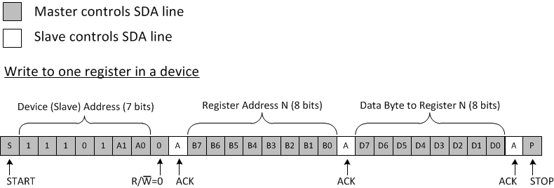 Figure 29. Write to Register
<br/>
 Figure 30. Write to the Polarity Inversion Register
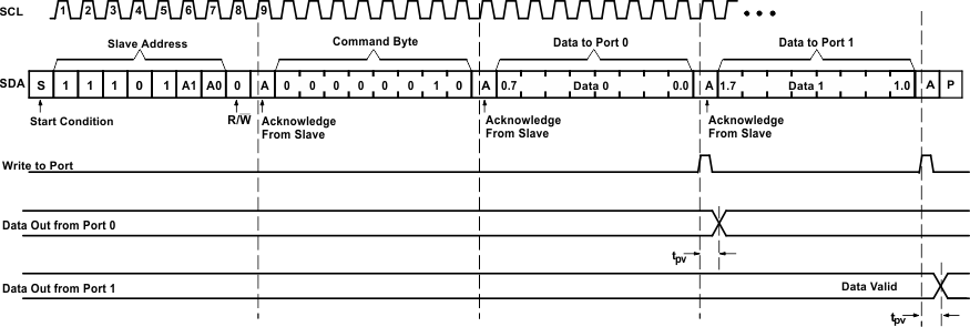 Figure 31. Write to Output Port Registers
8.6.3.1.2 Reads
Reading from a slave is very similar to writing, but requires some additional steps. In order to read from a slave, the master must first instruct the slave which register it wishes to read from. This is done by the master starting off the transmission in a similar fashion as the write, by sending the address with the R/W bit equal to 0 (signifying a write), followed by the register address it wishes to read from. When the slave acknowledges this register address, the master sends a START condition again, followed by the slave address with the R/W bit set to 1 (signifying a read). This time, the slave acknowledges the read request, and the master releases the SDA bus but continues supplying the clock to the slave. During this part of the transaction, the master becomes the master-receiver, and the slave becomes the slave-transmitter.
The master continues to send out the clock pulses, but releases the SDA line so that the slave can transmit data. At the end of every byte of data, the master sends an ACK to the slave, letting the slave know that it is ready for more data. When the master has received the number of bytes it is expecting, it sends a NACK, signaling to the slave to halt communications and release the bus. The master follows this up with a STOP condition.
See the Register Descriptions section for the list of the TCA9539s internal registers and a description of each one.
Figure 32 shows an example of reading a single byte from a slave register.
 Figure 32. Read from Register
After a restart, the value of the register defined by the command byte matches the register being accessed when the restart occurred. For example, if the command byte references Input Port 1 before the restart, the restart occurs when Input Port 0 is being read. The original command byte is forgotten. If a subsequent restart occurs, Input Port 0 is read first. Data is clocked into the register on the rising edge of the ACK clock pulse. After the first byte is read, additional bytes may be read, but the data now reflect the information in the other register in the pair. For example, if Input Port 1 is read, the next byte read is Input Port 0.
Data is clocked into the register on the rising edge of the ACK clock pulse. There is no limitation on the number of data bytes received in one read transmission, but when the final byte is received, the bus master must not acknowledge the data.
<br/>
