SCPS202C October 2009 – May 2016 TCA9539
PRODUCTION DATA.
- 1 Features
- 2 Applications
- 3 Description
- 4 Revision History
- 5 Pin Configuration and Functions
- 6 Specifications
- 7 Parameter Measurement Information
- 8 Detailed Description
- 9 Application and Implementation
- 10Power Supply Recommendations
- 11Layout
- 12Device and Documentation Support
- 13Mechanical, Packaging, and Orderable Information
7 Parameter Measurement Information

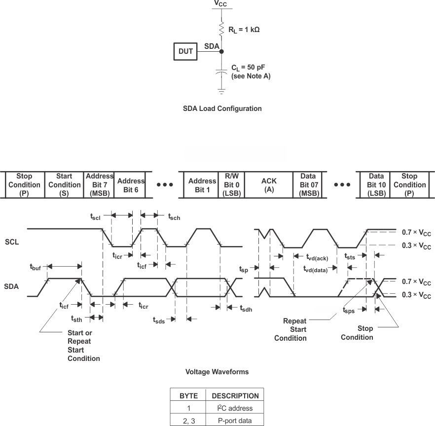
A. CL includes probe and jig capacitance.
B. All inputs are supplied by generators having the following characteristics: PRR ≤ 10 MHz, ZO = 50 Ω, tr/tf ≤ 30 ns.
C. All parameters and waveforms are not applicable to all devices.
Figure 19. I2C Interface Load Circuit and Voltage Waveforms

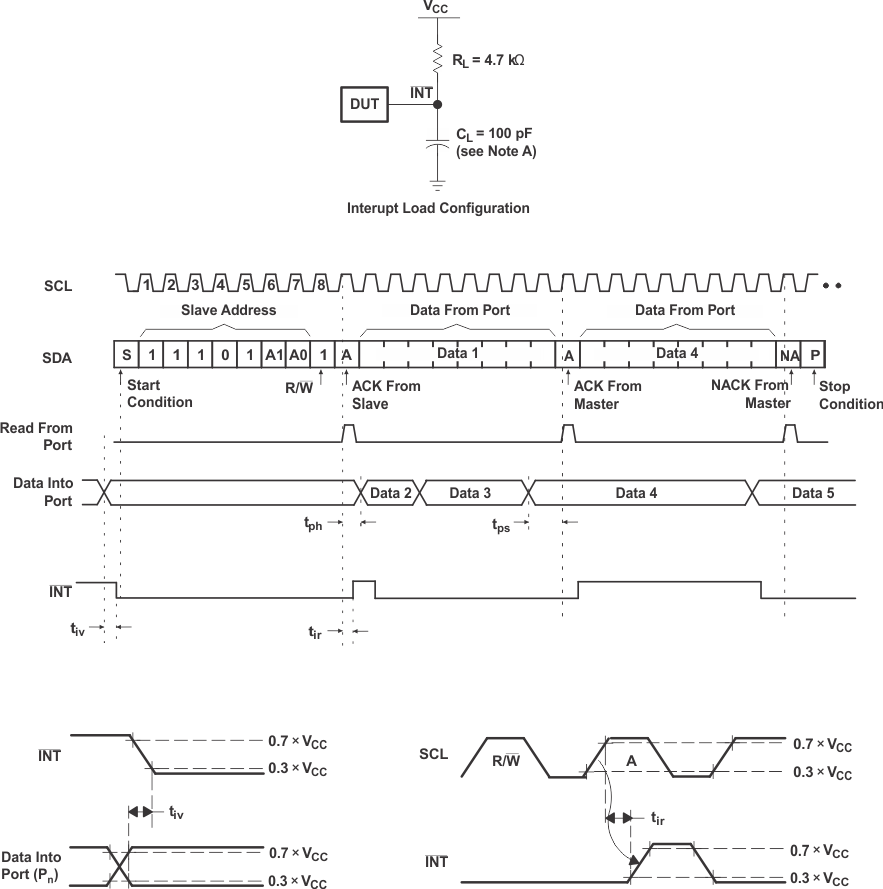
A. CL includes probe and jig capacitance.
B. All inputs are supplied by generators having the following characteristics: PRR ≤ 10 MHz, ZO = 50 Ω, tr/tf ≤ 30 ns.
C. All parameters and waveforms are not applicable to all devices.
Figure 20. Interrupt Load Circuit and Voltage Waveforms

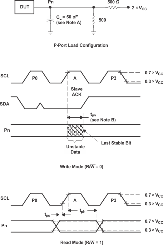
A. CL includes probe and jig capacitance.
B. tpv is measured from 0.7 × VCC on SCL to 50% I/O (Pn) output.
C. All inputs are supplied by generators having the following characteristics: PRR ≤ 10 MHz, ZO = 50 Ω, tr/tf ≤ 30 ns.
D. The outputs are measured one at a time, with one transition per measurement.
E. All parameters and waveforms are not applicable to all devices.
Figure 21. P-Port Load Circuit and Voltage Waveforms

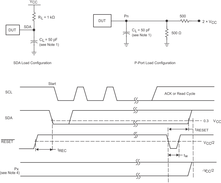
A. CL includes probe and jig capacitance.
B. All inputs are supplied by generators having the following characteristics: PRR ≤ 10 MHz, ZO = 50 Ω, tr/tf ≤ 30 ns.
C. The outputs are measured one at a time, with one transition per measurement.
D. I/Os are configured as inputs.
E. All parameters and waveforms are not applicable to all devices.
Figure 22. Reset Load Circuits and Voltage Waveforms