SFFS102 September 2021 SN74LVC3G07-Q1
4 Pin Failure Mode Analysis (Pin FMA)
This section provides a Failure Mode Analysis (FMA) for the pins of the SN74LVC3G07-Q1. The failure modes covered in this document include the typical pin-by-pin failure scenarios:
- Pin short-circuited to Ground (see Table 4-2)
- Pin open-circuited (see Table 4-3)
- Pin short-circuited to an adjacent pin (see Table 4-4)
- Pin short-circuited to VCC (see Table 4-5)
Table 4-2 through Table 4-5 also indicate how these pin conditions can affect the device as per the failure effects classification in Table 4-1.
Table 4-1 TI Classification of Failure
Effects
| Class | Failure Effects |
|---|---|
| A | Potential device damage that affects functionality |
| B | No device damage, but loss of functionality |
| C | No device damage, but performance degradation |
| D | No device damage, no impact to functionality or performance |
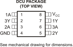
Figure 4-1 shows the SN74LVC3G07-Q1 pin diagram. For a detailed description of the device pins please refer to the Pin Configuration and Functions section in the SN74LVC3G07-Q1 data sheet.
 Figure 4-1 Pin Diagram
Table 4-2 Pin FMA for Device Pins
Short-Circuited to Ground
| Pin Name | Pin No. | Description of Potential Failure Effect(s) | Failure Effect Class |
|---|---|---|---|
| 1-3A | 6 | The input pin functionality is defined as low input (for example, if the buffer input is GND, then the output will always be driven low). | B |
| 1-3Y | 2 | If the buffer output is shorted to ground and is attempting to drive to VCC, then it can cause excessive output current, and the output will not switch. | A |
| VCC | 8 | The device is not powered, because short is external to the device. System level damage may occur in this scenario. | B |
| GND | 4 | Normal operation. | D |
Table 4-3 Pin FMA for Device Pins
Open-Circuited
| Pin Name | Pin No. | Description of Potential Failure Effect(s) | Failure Effect Class |
|---|---|---|---|
| 1-3A | 6 | The pin is floating, and it can change the output state and cause excessive current to flow from VCC to GND. Refer to the Implications of Slow or Floating CMOS Inputs section in the SN74LVC3G07-Q1 application note for more information. | A |
| 1-3Y | 2 | Normal operation. | D |
| VCC | 8 | The device is not powered. | B |
| GND | 4 | The device is not powered. | B |
Table 4-4 Pin FMA for Device Pins
Short-Circuited to Adjacent Pin
| Pin Name | Pin No. | Shorted to | Description of Potential Failure Effect(s) | Failure Effect Class |
|---|---|---|---|---|
| 1-3A | 6 | 1-3A | Two inputs shorted together will not cause damage unless there is an external bus contention that drives the input (such that VIL<Input Voltage<VIH), in which case excessive supply current to GND may cause damage. System level damage may occur in this scenario. | A |
| 1-3A | 6 | 1-3Y | Can cause excessive output current, output will not switch (for example, if inverter input is shorted to output). | A |
| 1-3A | 6 | GND | See Table 4-2 input response for more information. | A |
| 1-3A | 6 | VCC | See Table 4-5 input response for more information. | A |
| 1-3Y | 2 | 1-3Y | Can cause excessive output current, and the output will not switch (for example, if one output is driving to VCC and another output is driving to GND). | A |
| 1-3Y | 2 | GND | See Table 4-2 output response for more information. | A |
| 1-3Y | 2 | VCC | See Table 4-5 output response for more information. | A |
| GND | 4 | VCC | The device is not powered, because short is external to the device. System level damage may occur in this scenario. | B |
Table 4-5 Pin FMA for Device Pins
Short-Circuited to
VCC
| Pin Name | Pin No. | Description of Potential Failure Effect(s) | Failure Effect Class |
|---|---|---|---|
| 1-3A | 6 | The input pin functionality is defined as high input. For example, if the buffer input is VCC, then the output will always be driven high. | B |
| 1-3Y | 2 | Can cause excessive output current, and the output will not switch (for example, if the buffer output is shorted to VCC and is attempting to drive to GND). | A |
| VCC | 8 | Normal operation. | D |
| GND | 4 | The device is not powered, because short is external to the device. System level damage may occur in this scenario. | B |