SFFS106 November 2021 SN74LVC2G17-Q1
4 Pin Failure Mode Analysis (Pin FMA)
This section provides a Failure Mode Analysis (FMA) for the pins of the SN74LVC2G17-Q1. The failure modes covered in this document include the typical pin-by-pin failure scenarios:
- Pin short-circuited to Ground (see Table 4-2)
- Pin open-circuited (see Table 4-3)
- Pin short-circuited to an adjacent pin (see Table 4-4)
- Pin short-circuited to VCC (see Table 4-5)
Table 4-2 through Table 4-5 also indicate how these pin conditions can affect the device as per the failure effects classification in Table 4-1.
Table 4-1 TI Classification of Failure
Effects
| Class | Failure Effects |
|---|---|
| A | Potential device damage that affects functionality |
| B | No device damage, but loss of functionality |
| C | No device damage, but performance degradation |
| D | No device damage, no impact to functionality or performance |
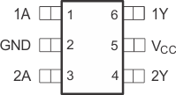
Figure 4-1 shows the SN74LVC2G17-Q1 pin diagram. For a detailed description of the device pins please refer to the Pin Configuration and Functions section in the SN74LVC2G17-Q1 data sheet.
 Figure 4-1 Pin Diagram
Table 4-2 Pin FMA for Device Pins
Short-Circuited to Ground
| Pin Name | Pin No. | Description of Potential Failure Effect(s) | Failure Effect Class |
|---|---|---|---|
| Input | 1, 3 | Input pin functionality is defined such as input is LOW – see the Device Functional Modes section in the SN74LVC2G17-Q1 Automotive Dual Schmitt-Trigger Buffer data sheet (for example, if buffer input is GND, then the output will always be driven LOW). | B |
| Output | 4, 6 | Can cause excessive output current and output will not switch (for example, if buffer output is shorted to ground and is attempting to drive to VCC). | A |
| VCC | 5 | Device will not be powered, because short is external to device; system level damage may occur in this scenario. | B |
| GND | 2 | Normal operation. | D |
Table 4-3 Pin FMA for Device Pins
Open-Circuited
| Pin Name | Pin No. | Description of Potential Failure Effect(s) | Failure Effect Class |
|---|---|---|---|
| Input | 1, 3 | Pin is floating; can change output state and cause excessive current from VCC to GND (See Implications of Slow or Floating CMOS Inputs) | A |
| Output | 4, 6 | Normal operation. | D |
| VCC | 5 | Device will not be powered. | B |
| GND | 2 | Device will not be powered. | B |
Table 4-4 Pin FMA for Device Pins
Short-Circuited to Adjacent Pin
| Pin Name | Pin No. | Shorted to | Description of Potential Failure Effect(s) | Failure Effect Class |
|---|---|---|---|---|
| Input | 1, 3 | Input | Two inputs shorted together will not cause damage unless there is an external bus contention that drives the input (such that VIL<Input Voltage<VIH) in which case excessive supply current to GND may cause damage; system level damage may occur in this scenario. | A |
| Input | 1, 3 | Output | Can cause excessive output current and output will not switch (for example, if inverter input is shorted to output). | A |
| Input | 1, 3 | GND | See input response in Table 4-2. | A |
| Input | 1, 3 | VCC | See input response in Table 4-5. | A |
| Output | 4, 6 | Output | Can cause excessive output current, and output will not switch (for example, if one output is driving to VCC and another output is driving to GND). | A |
| Output | 4, 6 | GND | See output response in Table 4-2. | A |
| Output | 4, 6 | VCC | See output response in Table 4-5. | A |
| GND | 2 | VCC | Device will not be powered, because short is external to the device; system level damage may occur in this scenario. | B |
Table 4-5 Pin FMA for Device Pins
Short-Circuited to
VCC
| Pin Name | Pin No. | Description of Potential Failure Effect(s) | Failure Effect Class |
|---|---|---|---|
| Input | 1, 3 | Input pin functionality is defined such as input is HIGH – see the Device Functional Modes section in the SN74LVC2G17-Q1 Automotive Dual Schmitt-Trigger Buffer data sheet (for example, if the buffer input is VCC, then the output will always be driven HIGH) | B |
| Output | 4, 6 | Can cause excessive output current and the output will not switch (for example, if the buffer output is shorted to VCC and is attempting to drive to GND). | A |
| VCC | 5 | Normal operation. | D |
| GND | 2 | Device will not be powered, because short is external to the device; system level damage may occur in this scenario. | B |