SFFS171 May 2021 TPS629203-Q1 , TPS629206-Q1 , TPS629210-Q1
3 Pin Failure Mode Analysis (Pin FMA)
This section provides a Failure Mode Analysis (FMA) for the pins of the TPS6292xx-Q1. The failure modes covered in this document include the typical pin-by-pin failure scenarios:
- Pin short-circuited to Ground (see Table 3-2)
- Pin open-circuited (see Table 3-3)
- Pin short-circuited to an adjacent pin (see Table 3-4)
- Pin short-circuited to VIN (see Table 3-5)
Table 3-2 through Table 3-5 also indicate how these pin conditions can affect the device as per the failure effects classification in Table 3-1.
| Class | Failure Effects |
|---|---|
| A | Potential device damage that affects functionality |
| B | No device damage, but loss of functionality |
| C | No device damage, but performance degradation |
| D | No device damage, no impact to functionality or performance |
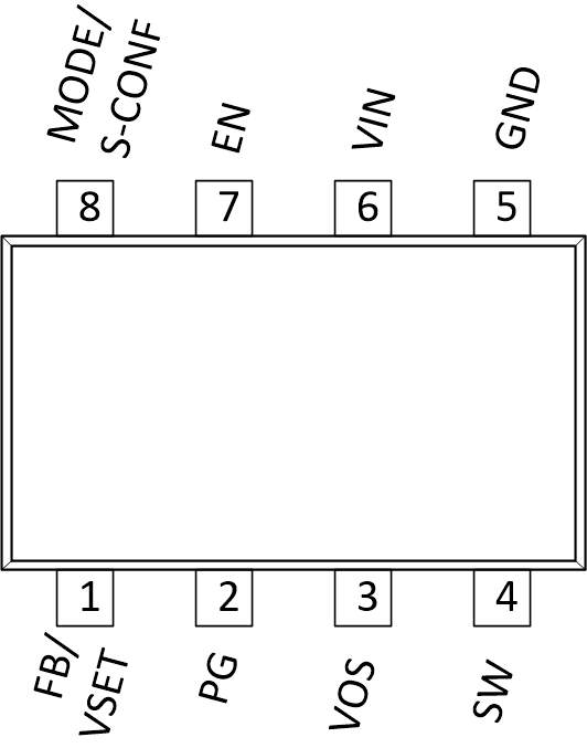
Figure 3-1 shows the TPS6292xx-Q1 pin diagram. For a detailed description of the device pins please refer to the 'Pin Configuration and Functions' section in the TPS6292xx-Q1 datasheet.
 Figure 3-1 PIin Diagram
Following are the assumptions of use and the device configuration assumed for the pin FMA in this section:
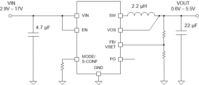
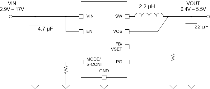
- The device is operating in one of the two typical application configurations show in Figure 3-2 or Figure 3-3.
 Figure 3-2 Adjustable VO Operation
Schematic
  Figure 3-3 Set-able VO Operation
Schematic
 | Pin Name | Pin No. | Application Configuration | Description of Potential Failure Effect(s) | Failure Effect Class |
|---|---|---|---|---|
| FB/VSET |
1 |
External FB(3) | Loss of output voltage
regualtion. Output voltage will go to Vin Possible device damge. (2) Abs Max voltage may be exceeded. |
A |
| Internal FB(4) | Device will regulate output voltage to 1.2V | D | ||
| PG |
2 |
Loss of PG functionality | C | |
| VOS |
3 |
Loss of output volatge | B | |
| SW |
4 |
Possible device damage | A | |
| GND |
5 |
Intended pin connection | D | |
| VIN |
6 |
Deice does not power on | B | |
| EN |
7 |
Device does not power on | B | |
| MODE/S-CONF |
8 |
External FB(3) | Part will run in 2.5MHz APFM with AEE mode(5) | C(5) |
| Internal FB(4) | Loss of output voltage
regualtion. Output voltage will go to Vin(5) Possible device damge. (2) Abs Max voltage may be exceeded. |
A(5) |
| Pin Name | Pin No. | Application Configuration | Description of Potential Failure Effect(s) | Failure Effect Class |
|---|---|---|---|---|
| FB/VSET |
1 |
External FB(3) | Loss of output voltage
regualtion. Output voltage may go to Vin Possible device damge. (2) Abs Max voltage may be exceeded. |
A |
| Internal FB(4) | Device will regulate output voltage to 3.3V | D | ||
| PG |
2 |
Loss of PG functionality | C | |
| VOS |
3 |
External FB(3) | Open loop operation. Undetermined outputt voltage behavior |
B |
| Internal FB(4) | Loss of output voltage
regualtion. Output voltage may go to Vin Possible device damge. (2) Abs Max may be exceeded. |
A | ||
| SW |
4 |
Loss of output voltage regulation | B | |
| GND |
5 |
Potential device damage | A | |
| VIN |
6 |
Device does not power on | B | |
| EN |
7 |
Device does not power on | B | |
| MODE/S-CONF |
8 |
External FB(3) | Part will run in 2.5MHz APFM with AEE mode(5) | C(5) |
| Internal FB(4) | Loss of output voltage
regualtion. Output voltage will go to Vin(5) Possible device damge. (2) Abs Max voltage may be exceeded. |
A(5) |
| Pin Name | Pin No. | Shorted to | Application Configuration | Description of Potential Failure Effect(s) | Failure Effect Class |
|---|---|---|---|---|---|
| FB/VSET | 1 | PG | Loss of output voltage
regualtion. Possible device damge(1). Abs Max voltage may be exceeded if PG is connected to Vin through a resitor. |
A | |
| PG | 2 | VOS | Loss of output voltage
regualtion. Possible device damge(1). Abs Max voltage may be exceeded if PG is connected to Vin through a resitor. |
A | |
| VOS | 3 | SW | Loss of output voltage
regualtion. Possible device damge(1). Abs Max volatge may be exceeded. |
A | |
| GND | 5 | VIN | Device not functional | B | |
| VIN | 6 | EN | Device cannot be disabled | B | |
| EN | 7 | MODE/S_CONF | External FB(3) | Part will run in 2.5MHz FPFM mode | C |
| Internal FB(4) | Loss of output voltage
regualtion. Output voltage will go to Vin(5) Possible device damge. (2) Abs Max voltage may be exceeded. |
A |
| Pin Name | Pin No. | Application Configuration | Description of Potential Failure Effect(s) | Failure Effect Class |
|---|---|---|---|---|
| FB/VSET |
1 |
Possible device damge(1). Abs Max volatge may be exceeded. | A | |
| PG |
2 |
Potential device damage. Abs Max current rating for pin | A | |
| VOS |
3 |
Possible device damge(1). Abs Max volatge may be exceeded. | A | |
| SW |
4 |
Possible device damge. (2) Abs Max voltage may be exceeded. | A | |
| GND |
5 |
Device not functional | B | |
| VIN |
6 |
Intended pin connection | D | |
| EN |
7 |
Device cannot be disabled | B | |
| MODE/S-CONF |
8 |
External FB(3) | Part will run in 2.5MHz FPFM mode (5) | C(5) |
| Internal FB(4) | Loss of output voltage
regualtion. Output voltage will go to Vin(5) Possible device damge. (2) Abs Max voltage may be exceeded. |
A(5) |