SFFS220 September 2021 TVS3301
4 Pin Failure Mode Analysis (Pin FMA)
This section provides a Failure Mode Analysis (FMA) for the pins of the TVS3301. The failure modes covered in this document include the typical pin-by-pin failure scenarios:
- Pin short-circuited to Ground (see Table 4-2)
- Pin open-circuited (see Table 4-3)
- Pin short-circuited to an adjacent pin (see Table 4-4)
Table 4-2 through Table 4-4 also indicate how these pin conditions can affect the device as per the failure effects classification in Table 4-1.
Table 4-1 TI Classification of Failure
Effects
| Class | Failure Effects |
|---|---|
| A | Potential device damage that affects functionality. |
| B | No device damage, but loss of functionality. |
| C | No device damage, but performance degradation. |
| D | No device damage. No impact to functionality or performance. |
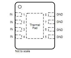
Figure 4-1 shows the TVS3301 pin diagram. For a detailed description of the device pins please refer to the Pin Configuration and Functions section in the TVS3301 data sheet.
 Figure 4-1 Pin Diagram
Following are the assumptions of use and the device configuration assumed for the pin FMA in this section:
- The DC signal on the protected line does not go above 33 V.
- All other pins are connected properly for each case.
- The slew rate of the signal on the protected line is below the specified limits according to the data sheet.
Table 4-2 Pin FMA for Device Pins
Short-Circuited to Ground
| Pin Name | Pin No. | Description of Potential Failure Effect(s) | Failure Effect Class |
|---|---|---|---|
| IN | 1 | Signal of protected line would be shorted to ground. | B |
| IN | 2 | Signal of protected line would be shorted to ground. | B |
| IN | 3 | Signal of protected line would be shorted to ground. | B |
| IN | 4 | Signal of protected line would be shorted to ground. | B |
| GND | 5 | No effect; normal operation. | D |
| GND | 6 | No effect; normal operation. | D |
| GND | 7 | No effect; normal operation. | D |
| GND | 8 | No effect; normal operation. | D |
Table 4-3 Pin FMA for Device Pins
Open-Circuited
| Pin Name | Pin No. | Description of Potential Failure Effect(s) | Failure Effect Class |
|---|---|---|---|
| IN | 1 | No effect. | D |
| IN | 2 | No effect. | D |
| IN | 3 | No effect. | D |
| IN | 4 | No effect. | D |
| GND | 5 | No effect. | D |
| GND | 6 | No effect. | D |
| GND | 7 | No effect. | D |
| GND | 8 | No effect. | D |
Table 4-4 Pin FMA for Device Pins
Short-Circuited to Adjacent Pin
| Pin Name | Pin No. | Shorted to | Description of Potential Failure Effect(s) | Failure Effect Class |
|---|---|---|---|---|
| IN | 1 | 2 | No effect; normal operation. | D |
| IN | 2 | 3 | No effect; normal operation. | D |
| IN | 3 | 4 | No effect; normal operation. | D |
| GND | 5 | 6 | No effect; normal operation. | D |
| GND | 6 | 7 | No effect; normal operation. | D |
| GND | 7 | 8 | No effect; normal operation. | D |