SFFS221 September 2021 TVS1401
4 Pin Failure Mode Analysis (Pin FMA)
This section provides a Failure Mode Analysis (FMA) for the pins of the TVS1401. The failure modes covered in this document include the typical pin-by-pin failure scenarios:
- Pin short-circuited to Ground (see Table 4-2)
- Pin open-circuited (see Table 4-3)
- Pin short-circuited to an adjacent pin (see Table 4-4)
Table 4-2 through Table 4-4 also indicate how these pin conditions can affect the device as per the failure effects classification in Table 4-1.
| Class | Failure Effects |
|---|---|
| A | Potential device damage that affects functionality. |
| B | No device damage, but loss of functionality. |
| C | No device damage, but performance degradation. |
| D | No device damage. No impact to functionality or performance. |
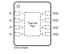
Figure 4-1 shows the TVS1401 pin diagram. For a detailed description of the device pins please refer to the Pin Configuration and Functions section in the TVS1401 data sheet.
 Figure 4-1 Pin Diagram
Following are the assumptions of use and the device configuration assumed for the pin FMA in this section:
The DC signal on the protected line does not go above 14 V.
All other pins are connected properly for each case.
The slew rate of the signal on the protected line is below the specified limits according to the data sheet.
| Pin Name | Pin No. | Description of Potential Failure Effect(s) | Failure Effect Class |
|---|---|---|---|
| IN | 1 | Signal of protected line would be shorted to ground. | B |
| IN | 2 | Signal of protected line would be shorted to ground. | B |
| IN | 3 | Signal of protected line would be shorted to ground. | B |
| IN | 4 | Signal of protected line would be shorted to ground. | B |
| GND | 5 | No effect; normal operation. | D |
| GND | 6 | No effect; normal operation. | D |
| GND | 7 | No effect; normal operation. | D |
| GND | 8 | No effect; normal operation. | D |
| Pin Name | Pin No. | Description of Potential Failure Effect(s) | Failure Effect Class |
|---|---|---|---|
| IN | 1 | No effect. | D |
| IN | 2 | No effect. | D |
| IN | 3 | No effect. | D |
| IN | 4 | No effect. | D |
| GND | 5 | No effect. | D |
| GND | 6 | No effect. | D |
| GND | 7 | No effect. | D |
| GND | 8 | No effect. | D |
| Pin Name | Pin No. | Shorted to | Description of Potential Failure Effect(s) | Failure Effect Class |
|---|---|---|---|---|
| IN | 1 | 2 | No effect; normal operation. | D |
| IN | 2 | 3 | No effect; normal operation. | D |
| IN | 3 | 4 | No effect; normal operation. | D |
| GND | 5 | 6 | No effect; normal operation. | D |
| GND | 6 | 7 | No effect; normal operation. | D |
| GND | 7 | 8 | No effect; normal operation. | D |