SFFS252 august 2023 TLV1851 , TLV1851-Q1 , TLV1861 , TLV1861-Q1
5 Pin Failure Mode Analysis (Pin FMA)
This section provides a Failure Mode Analysis (FMA) for the pins of the TLV1852-Q1 and TLV1862-Q1. The failure modes covered in this document include the typical pin-by-pin failure scenarios:
- Pin short-circuited to V- (see Table 5-2)
- Pin open-circuited (see Table 5-3)
- Pin short-circuited to an adjacent pin (see Table 5-4)
- Pin short-circuited to V+ (see Table 5-5)
Table 5-2 through Table 5-5 also indicate how these pin conditions can affect the device as per the failure effects classification in Table 5-1.
| Class | Failure Effects |
|---|---|
| A | Potential device damage that affects functionality |
| B | No device damage, but loss of functionality |
| C | No device damage, but performance degradation |
| D | No device damage, no impact to functionality or performance |
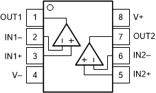
Figure 5-1 shows the TLV1852-Q1 and TLV1862-Q1 pin diagram. For a detailed description of the device pins please refer to the Pin Configuration and Functions section in the TLV1852-Q1 and TLV1862-Q1 data sheet.
 Figure 5-1 Pin Diagram
Following are the assumptions of use and the device configuration assumed for the pin FMA in this section:
- Each pin is assessed individually
- All other pins are configured correctly for device functionality
| Pin Name | Pin No. | Description of Potential Failure Effect(s) | Failure Effect Class |
|---|---|---|---|
OUT1 | 1 | Thermal stress due to high power dissipation (Push-Pull) No change if same node as V- (Open-Drain) | A B |
IN1- | 2 | Output goes high, if other input is positive | B |
IN1+ | 3 | Output goes low, if other input is positive | B |
V- | 4 | No change if same node as V- | D |
IN2+ | 5 | Output goes low, if other input is positive | B |
IN2- | 6 | Output goes high, if other input is positive | B |
OUT2 | 7 | Thermal stress due to high power dissipation (Push-Pull) No change if same node as V- (Open-Drain) | A B |
V+ | 8 | Main supply shorted out (no power to device) | B |
| Pin Name | Pin No. | Description of Potential Failure Effect(s) | Failure Effect Class |
|---|---|---|---|
OUT1 | 1 | Output can't drive application load | B |
IN1- | 2 | Output may be low or high | B |
IN1+ | 3 | Output may be low or high | B |
V- | 4 | Highest voltage pin will drive V- pin internally (via diode) | B |
IN2+ | 5 | Output may be low or high | B |
IN2- | 6 | Output may be low or high | B |
OUT2 | 7 | Output can't drive application load | B |
V+ | 8 | Main supply open (no power to device) | B |
| Pin Name | Pin No. | Shorted to | Description of Potential Failure Effect(s) | Failure Effect Class |
|---|---|---|---|---|
OUT1 to IN1- | 1 | 2 | Output may be low or high | B |
IN1- to IN1+ | 2 | 3 | Output may be low or high | B |
IN1+ to V- | 3 | 4 | Output goes low, if other input is positive | B |
V- to IN2+ | 4 | 5 | Output goes low, if other input is positive | B |
IN2+ to IN2- | 5 | 6 | Output may be low or high | B |
In2- to OUT2 | 6 | 7 | Output may be low or high | B |
OUT2 to V+ | 7 | 8 | Thermal stress due to high power dissipation | A |
V+ to OUT1 | 8 | 1 | Thermal stress due to high power dissipation | A |
| Pin Name | Pin No. | Description of Potential Failure Effect(s) | Failure Effect Class |
|---|---|---|---|
OUT1 | 1 | Thermal stress due to high power dissipation | A |
IN1- | 2 | Output goes low, if other input is less positive | B |
IN1+ | 3 | Output goes high, if other input is less positive | B |
V- | 4 | Main supply shorted out (no power to device) | B |
IN2+ | 5 | Output goes high, if other input is less positive | B |
IN2- | 6 | Output goes low, if other input is less positive | B |
| OUT2 | 7 | Thermal stress due to high power dissipation | A |
| V+ | 8 | No change if same node as V+ | D |