SFFS285 January 2024 LM74701-Q1
4 Pin Failure Mode Analysis (Pin FMA)
This section provides a Failure Mode Analysis (FMA) for the pins of the LM74701-Q1. The failure modes covered in this document include the typical pin-by-pin failure scenarios:
- Pin short-circuited to Ground (see Table 4-2)
- Pin open-circuited (see Table 4-3)
- Pin short-circuited to an adjacent pin (see Table 4-4)
- Pin short-circuited to supply (see Table 4-5)
Table 4-2 through Table 4-5 also indicate how these pin conditions can affect the device as per the failure effects classification in Table 4-1.
| Class | Failure Effects |
|---|---|
| A | Potential device damage that affects functionality |
| B | No device damage, but loss of functionality |
| C | No device damage, but performance degradation |
| D | No device damage, no impact to functionality or performance |
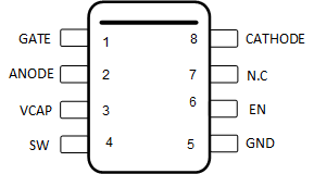
Figure 4-1 shows the LM74701-Q1 pin diagram. For a detailed description of the device pins please refer to the Pin Configuration and Functions section in the LM74701-Q1 data sheet.
 Figure 4-1 LM74701-Q1 Pin Diagram
| Pin Name | Pin No. | Description of Potential Failure Effect(s) | Failure Effect Class |
|---|---|---|---|
|
GATE |
1 |
Device can get damaged due to internal conduction path from ANODE to GATE. |
A |
|
ANODE |
2 |
Device will not power up. Equivalent to input supply shorted to GND. |
B |
|
VCAP |
3 |
Device can get damaged due to internal conduction path from ANODE to VCAP. |
A |
|
SW |
4 |
Device can get damaged due to internal switch conduction when EN pin is high. |
A |
|
GND |
5 |
No effect on the device behavior. |
D |
|
EN |
6 |
Device will be in shutdown mode. External MOSFET will not turn on. |
B |
|
N.C |
7 |
No effect on the device behavior. |
D |
|
CATHODE |
8 |
VDS clamp feature will not be functional. |
B |
| Pin Name | Pin No. | Description of Potential Failure Effect(s) | Failure Effect Class |
|---|---|---|---|
|
GATE |
1 |
External FET will not turn on. |
B |
|
ANODE |
2 |
Device will not power up. |
B |
|
VCAP |
3 |
Charge pump voltage will not be available. External FET will not turn on. |
B |
|
SW |
4 |
No effect on the device behavior. |
D |
|
GND |
5 |
Device may not power up. |
B |
|
EN |
6 |
Device will be in shutdown mode due to internal pull down on EN pin. |
B |
|
N.C |
7 |
No effect on the device behavior. |
D |
|
CATHODE |
8 |
VDS clamp feature and reverse current blocking feature will not be functional. |
B |
| Pin Name | Pin No. | Shorted to | Description of Potential Failure Effect(s) | Failure Effect Class |
|---|---|---|---|---|
|
GATE |
1 |
ANODE |
External FET will not turn on. Device quiescent current may increase. |
B |
|
ANODE |
2 |
VCAP |
External FET will not turn on. Device quiescent current may increase. |
B |
|
VCAP |
3 |
SW |
External FET may not turn on due to VCAP loading, when external resistor divider connected from SW pin to GND. |
B |
|
SW |
4 |
— |
SW is the corner pin. No effect on the device performance. |
D |
|
GND |
5 |
EN |
Device will be in shutdown mode. |
B |
|
EN |
6 |
N.C |
No effect on the device performance. |
D |
|
N.C |
7 |
CATHODE |
No effect on the device performance. |
D |
|
CATHODE |
8 |
— |
Corner pin. No effect on the device performance. |
D |
| Pin Name | Pin No. | Description of Potential Failure Effect(s) | Failure Effect Class |
|---|---|---|---|
|
GATE |
1 |
External FET will not turn on. |
B |
|
ANODE |
2 |
No effect on the device performance. |
D |
|
VCAP |
3 |
Charge pump voltage will not be available. External FET will not turn on. |
B |
|
SW |
4 |
Battery voltage monitoring will be always available, irrespective of EN pin status. |
B |
|
GND |
5 |
Device will not power up as supply is shorted to GND. |
B |
|
EN |
6 |
Device will be in always on mode. |
B |
|
N.C |
7 |
No effect on the device performance. |
D |
|
CATHODE |
8 |
External FET is bypassed. Reverse current blocking and VDS clamp feature will not be functional. |
B |