SFFS317A December 2021 – April 2022 BQ77207
4 Pin Failure Mode Analysis (Pin FMA)
This section provides a Failure Mode Analysis (FMA) for the pins of the BQ77207. The failure modes covered in this document include the typical pin-by-pin failure scenarios:
- Pin short-circuited to Ground (see Table 4-2)
- Pin open-circuited (see Table 4-3)
- Pin short-circuited to an adjacent pin (see Table 4-4)
- Pin short-circuited to supply (see Table 4-5)
Table 4-2 through Table 4-5 also indicate how these pin conditions can affect the device as per the failure effects classification in Table 4-1.
Table 4-1 TI Classification of Failure Effects
| Class | Failure Effects |
|---|---|
| A | Potential device damage that affects functionality |
| B | No device damage, but loss of functionality |
| C | No device damage, but performance degradation |
| D | No device damage, no impact to functionality or performance |
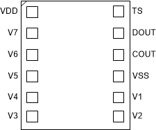
Figure 4-1 shows the BQ77207 pin diagram. For a detailed description of the device pins please refer to the Pin Configuration and Functions section in the BQ77207 data sheet.
 Figure 4-1 Pin Diagram
Table 4-2 Pin FMA for Device Pins Short-Circuited to Ground
| Pin Name | Pin No. | Description of Potential Failure Effect(s) | Failure Effect Class |
|---|---|---|---|
| VDD | 1 | No power to part | B |
| V7 | 2 | Automatic OV detection. | D |
| V6 | 3 | Automatic OV detection. | D |
| V5 | 4 | Automatic OV detection. | D |
| V4 | 5 | Automatic OV detection. | D |
| V3 | 6 | Automatic OV detection. | D |
| V2 | 7 | Automatic OV detection. | D |
| V1 | 8 | Automatic OV detection. | D |
| VSS | 9 | Function as normal | D |
| COUT | 10 | No output signal to system | B |
| DOUT | 11 | No output signal to system | B |
| TS | 12 | Automatic OT detection. | D |
Table 4-3 Pin FMA for Device Pins Open-Circuited
| Pin Name | Pin No. | Description of Potential Failure Effect(s) | Failure Effect Class |
|---|---|---|---|
| VDD | 1 | No power to part | B |
| V7 | 2 | Automatic OW detection. | D |
| V6 | 3 | Automatic OW detection. | D |
| V5 | 4 | Automatic OW detection. | D |
| V4 | 5 | Automatic OW detection. | D |
| V3 | 6 | Automatic OW detection. | D |
| V2 | 7 | Automatic OW detection. | D |
| V1 | 8 | Automatic OW detection. | D |
| VSS | 9 | No power to part | B |
| COUT | 10 | No output signal to system | B |
| DOUT | 11 | No output signal to system | B |
| TS | 12 | No OT detection. | B |
Table 4-4 Pin FMA for Device Pins Short-Circuited to Adjacent Pin
| Pin Name | Pin No. | Shorted to | Description of Potential Failure Effect(s) | Failure Effect Class |
|---|---|---|---|---|
| VDD | 1 | V7 | Function as normal | C |
| V7 | 2 | VDD | Function as normal | C |
| V6 | 3 | V7 | Automatic OV detection. | D |
| V5 | 4 | V6 | Automatic OV detection. | D |
| V4 | 5 | NC | Function as normal | D |
| V3 | 6 | V4 | Automatic OV detection | D |
| V2 | 7 | V3 | Automatic OV detection. | D |
| V1 | 8 | V2 | Automatic OV detection. | D |
| VSS | 9 | V1 | Automatic OV detection. | D |
| COUT | 10 | VSS | No output signal to system | B |
| DOUT | 11 | COUT | No output signal to system | B |
| TS | 12 | DOUT | Automatic OT detection. | D |
Table 4-5 Pin FMA for Device Pins Short-Circuited to Supply
| Pin Name | Pin No. | Description of Potential Failure Effect(s) | Failure Effect Class |
|---|---|---|---|
| VDD | 1 | Function as normal | C |
| V7 | 2 | AFunction as normal | C |
| V6 | 3 | Automatic OV detection. | D |
| V5 | 4 | Automatic OV detection. | D |
| V4 | 5 | Automatic OV detection. | D |
| V3 | 6 | Automatic OV detection. | D |
| V2 | 7 | Automatic OV detection. | D |
| V1 | 8 | Automatic OV detection. | D |
| VSS | 9 | Automatic OW detection. | D |
| COUT | 10 | No output signal to system | B |
| DOUT | 11 | No output signal to system | B |
| TS | 12 | No OT detection. | A |