SFFS358 September 2022 TPS784-Q1
4.1 VSON Package
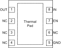
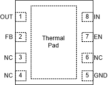
Figure 4-1 shows the TPS784-Q1 pin diagram for the VSON package with a fixed output, and Figure 4-2 shows the TPS784-Q1 pin diagram for the VSON with an adjustable output. For a detailed description of the device pins, see the Pin Configuration and Functions section in the TPS784-Q1 data sheet.
 Figure 4-1 Pin Diagram
 (VSON Package), Fixed Version
 Figure 4-2 Pin Diagram
 (VSON Package), Adjustable Version
| Pin Name | Pin No. | Description of Potential Failure Effects | Failure Effect Class |
|---|---|---|---|
| OUT | 1 | Regulation is not possible, the device operates at current limit. The device can cycle in and out of thermal shutdown. | B |
| NC/FB | 2 |
(Fixed output.) No effect. Normal operation. (Adjustable output.) Output voltage is input voltage minus dropout voltage because the error amplifier drives the pass transistor gate to the rail. |
D/B |
| NC | 3 | No effect. Normal operation. | D |
| NC | 4 | No effect. Normal operation. | D |
| GND | 5 | No effect. Normal operation. | D |
| NC | 6 | No effect. Normal operation. | D |
| EN | 7 | The device is disabled, resulting in no output voltage. | B |
| IN | 8 | Power is not supplied to the device, resulting in no output voltage. | B |
| Pin Name | Pin No. | Description of Potential Failure Effects | Failure Effect Class |
|---|---|---|---|
| OUT | 1 | The device output is disconnected from the load. | B |
| NC/FB | 2 |
(Fixed output.) No effect. Normal operation. (Adjustable output.) The error amplifier input is not connected. The output voltage is indeterminate. |
D/B |
| NC | 3 | No effect. Normal operation. | D |
| NC | 4 | No effect. Normal operation. | D |
| GND | 5 | There is no current loop for the supply voltage. The device is not operational and does not regulate. | B |
| NC | 6 | No effect. Normal operation. | D |
| EN | 7 | The enable circuit is in an unknown state. The device can be enabled or disabled. | B |
| IN | 8 | Power is not supplied to the device, resulting in no output voltage. | B |
| Pin Name | Pin No. | Shorted to | Description of Potential Failure Effects | Failure Effect Class |
|---|---|---|---|---|
| OUT | 1 | NC/FB (pin 2) |
(Fixed output.) No effect. Normal operation. (Adjustable output.) The output voltage is set to the internal reference voltage. |
D/B |
| FB | 2 | NC (pin 3) | No effect. Normal operation. | D |
| NC | 3 | NC (pin 4) | No effect. Normal operation. | D |
| GND | 5 | NC (pin 6) | No effect. Normal operation. | D |
| NC | 6 | EN (pin 7) | No effect. Normal operation. | D |
| EN | 7 | IN (pin 8) | The device is always enabled. Peripherals connected to EN can be at risk of EOS. | B |
| Pin Name | Pin No. | Description of Potential Failure Effects | Failure Effect Class |
|---|---|---|---|
| OUT | 1 | The device does not regulate. | B |
| NC/FB | 2 |
(Fixed output.) No effect. Normal operation. (Adjustable output.) The absolute maximum rating for the FB pin (2 V max) can be violated, resulting in the device being destroyed. If the absolute maximum rating is not violated, the error amplifier closes the channel and there is no output voltage. |
D/A |
| NC | 3 | No effect. Normal operation. | D |
| NC | 4 | No effect. Normal operation. | D |
| GND | 5 | No output voltage. System performance depends on upstream overcurrent protection. | B |
| NC | 6 | No effect. Normal operation. | D |
| EN | 7 | The device is always enabled. | B |
| IN | 8 | No effect. Normal operation. | D |