SFFS493 October 2024 OPT4001-Q1
4 Pin Failure Mode Analysis (Pin FMA)
This section provides a failure mode analysis (FMA) for the pins of the OPT4001-Q1. The failure modes covered in this document include the typical pin-by-pin failure scenarios:
- Pin short-circuited to ground (see Table 4-2)
- Pin open-circuited (see Table 4-3)
- Pin short-circuited to an adjacent pin (see Table 4-4)
- Pin short-circuited to supply (see Table 4-5)
Table 4-2 through Table 4-5 also indicate how these pin conditions can affect the device as per the failure effects classification in Table 4-1.
Table 4-1 TI Classification of Failure Effects
| Class | Failure Effects |
|---|---|
| A | Potential device damage that affects functionality. |
| B | No device damage, but loss of functionality. |
| C | No device damage, but performance degradation. |
| D | No device damage, no impact to functionality or performance. |
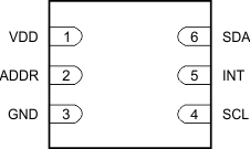
Figure 4-1 shows the OPT4001-Q1 pin diagram. For a detailed description of the device pins, see the Pin Configuration and Functions section in the OPT4001-Q1 data sheet.
 Figure 4-1 OPT4001-Q1
USON(6) Pin Diagram
Figure 4-1 OPT4001-Q1
USON(6) Pin DiagramFollowing are the assumptions of use and the device configuration assumed for the pin FMA in this section:
- Device is the only target on the I2C bus
- External pull-up resistor on SCL and SDA pins
Table 4-2 Pin FMA for Device Pins Short-Circuited to Ground
| Pin Name | Pin No. | Description of Potential Failure Effects | Failure Effect Class |
|---|---|---|---|
| VDD | 1 | Device is not powered. Device is not functional. Observe that the absolute maximum ratings for all pins of the device are met, otherwise device damage is plausible. | A |
| ADDR | 2 | Limited I2C address selection. Communication can be corrupted. | B |
| GND | 3 | No Effect. Normal Operation. | D |
| SCL | 4 | No I2C communication with the device is possible. | B |
| INT | 5 | Limited functionality of the device. Interrupt generation mechanism does not function and the device cannot indicate completion of conversion. | B |
| SDA | 6 | No I2C communication with the device is possible. | B |
Table 4-3 Pin FMA for Device Pins
Open-Circuited
| Pin Name | Pin No. | Description of Potential Failure Effects | Failure Effect Class |
|---|---|---|---|
| VDD | 1 | Device functionality is undetermined. Device is not powered if all external analog and digital pins are held low. | B |
| ADDR | 2 | Limited address selection. I2C communication can be corrupted. | B |
| GND | 3 | Device functionality is undetermined. Device can be not powered or connected to GND internally through an alternate pin ESD diode and power up. | B |
| SCL | 4 | No I2C communication with the device is possible. | B |
| INT | 5 | Limited functionality of the device. Interrupt generation mechanism does not function and the device cannot indicate completion of conversion. | B |
| SDA | 6 | No I2C communication with the device is possible. | B |
Table 4-4 Pin FMA for Device Pins Short-Circuited to Adjacent Pin
| Pin Name | Pin No. | Shorted to | Description of Potential Failure Effects | Failure Effect Class |
|---|---|---|---|---|
| VDD | 1 | ADDR | Limited I2C address selection. Communication can be corrupted. | B |
| ADDR | 2 | GND | Limited I2C address selection. Communication can be corrupted. | B |
| SCL | 4 | INT | I2C communication can be corrupted. Limited functionality of the device. Interrupt generation mechanism does not function and the device cannot indicate completion of conversion. | B |
| INT | 5 | SDA | I2C communication can be corrupted. Limited functionality of the device. Interrupt generation mechanism does not function and the device cannot indicate completion of conversion. | B |
Table 4-5 Pin FMA for Device Pins Short-Circuited to
Supply
| Pin Name | Pin No. | Description of Potential Failure Effects | Failure Effect Class |
|---|---|---|---|
| VDD | 1 | No Effect. Normal Operation. | D |
| ADDR | 2 | Limited I2C address selection. Communication can be corrupted. | B |
| GND | 3 | Device functionality is undetermined. Device is not powered if all external analog and digital pins are held low. Device can power up through internal ESD diodes to VDD if voltages are above the power-on reset threshold of the device and present on any of the analog or digital pins. | B |
| SCL | 4 | No I2C communication with device is possible. | B |
| INT | 5 | Limited functionality of the device. Interrupt generation mechanism does not function and the device cannot indicate completion of conversion. | B |
| SDA | 6 | No I2C communication with the device is possible. | B |