SFFS571 February 2023 TPS7B83-Q1
4 Pin Failure Mode Analysis (Pin FMA)
This section provides a failure mode analysis (FMA) for the pins of the TPS7B83-Q1. The failure modes covered in this document include the typical pin-by-pin failure scenarios:
- Pin short-circuited to ground (see Table 4-2)
- Pin open-circuited (see Table 4-3)
- Pin short-circuited to an adjacent pin (see Table 4-4)
- Pin short-circuited to supply (see Table 4-5)
Table 4-2 through Table 4-5 also indicate how these pin conditions can affect the device as per the failure effects classification in Table 4-1.
Table 4-1 TI Classification of Failure
Effects
| Class | Failure Effects |
|---|---|
| A | Potential device damage that affects functionality. |
| B | No device damage, but loss of functionality. |
| C | No device damage, but performance degradation. |
| D | No device damage, no impact to functionality or performance. |
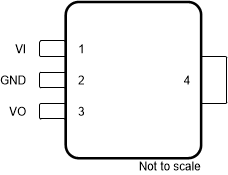
Figure 4-1 shows the TPS7B83-Q1 pin diagram. For a detailed description of the device pins, see the Pin Configuration and Functions section in the TPS7B83-Q1 data sheet.
 Figure 4-1 Pin Diagram
Table 4-2 Pin FMA for Device Pins
Short-Circuited to Ground
| Pin Name | Pin No. | Description of Potential Failure Effects | Failure Effect Class |
|---|---|---|---|
| IN | 1 | No output voltage. System performance depends on upstream current limiting. | B |
| GND | 2 | No effect. Normal operation. | D |
| OUT | 3 | Current limit is triggered, and the device can repeatedly enter and exit thermal shutdown depending on power dissipation. | B |
| GND | 4 | No effect. Normal operation. | D |
Table 4-3 Pin FMA for Device Pins
Open-Circuited
| Pin Name | Pin No. | Description of Potential Failure Effects | Failure Effect Class |
|---|---|---|---|
| IN | 1 | Power is not supplied to the device, resulting in no output voltage. | B |
| GND | 2 | A floating GND pin can result in incorrect voltage regulation or no output voltage. | B |
| OUT | 3 | The output is disconnected from the load. | B |
| GND | 4 | A floating GND pin can result in incorrect voltage regulation or no output voltage. | B |
Table 4-4 Pin FMA for Device Pins
Short-Circuited to Adjacent Pin
| Pin Name | Pin No. | Shorted to | Description of Potential Failure Effects | Failure Effect Class |
|---|---|---|---|---|
| IN | 1 | GND | No output voltage. System performance depends on upstream current limiting. | B |
| GND | 2 | OUT | Current limit is triggered, and the device can repeatedly enter and exit thermal shutdown depending on power dissipation. | B |
| OUT | 3 | GND | Current limit is triggered, and the device can repeatedly enter and exit thermal shutdown depending on power dissipation. | B |
Table 4-5 Pin FMA for Device Pins
Short-Circuited to
Supply
| Pin Name | Pin No. | Description of Potential Failure Effects | Failure Effect Class |
|---|---|---|---|
| IN | 1 | No effect. Normal operation. | D |
| GND | 2 | No output voltage. System performance depends on upstream current limiting. | B |
| OUT | 3 | The output is not regulated. VOUT = VIN. The OUT pin can be damaged if the absolute maximum rating (7 V) is violated. | B/A |
| GND | 4 | No output voltage. System performance depends on upstream current limiting. | B |