SFFS913 July 2024 TL1963A-Q1
4 Pin Failure Mode Analysis (Pin FMA)
This section provides a failure mode analysis (FMA) for the pins of the TL1963A-Q1. The failure modes covered in this document include the typical pin-by-pin failure scenarios:
- Pin short-circuited to ground (see Table 4-2)
- Pin open-circuited (see Table 4-3)
- Pin short-circuited to an adjacent pin (see Table 4-4)
Table 4-2 through Table 4-4 also indicate how these pin conditions can affect the device as per the failure effects classification in Table 4-1.
Table 4-1 TI Classification of Failure Effects
| Class | Failure Effects |
|---|---|
| A | Potential device damage that affects functionality. |
| B | No device damage, but loss of functionality. |
| C | No device damage, but performance degradation. |
| D | No device damage, no impact to functionality or performance. |
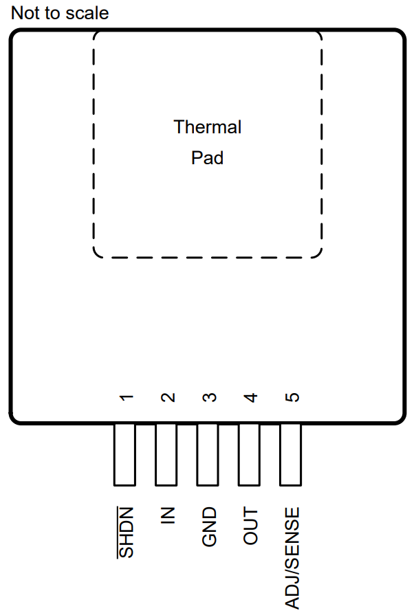
Figure 4-1 shows the TL1963A-Q1 pin diagram. For a detailed description of the device pins, see the Pin Configuration and Functions section in the TL1963A-Q1 data sheet.
 Figure 4-1 Pin Diagram
Table 4-2 Pin FMA for Device Pins Short-Circuited to
Ground
| Pin Name | Pin No. | Description of Potential Failure Effects | Failure Effect Class |
|---|---|---|---|
| SHDN | 1 | Output is off when pin is pulled low. | B |
| IN | 2 | No input to the device, potential damage to upstream supply. | B |
| GND | 3 | No effect. | D |
| OUT | 4 | Output voltage is at, or near, ground. The device is in current limit. The device can cycle in and out of thermal shutdown depending on power dissipation. | B |
| ADJ/SENSE | 5 | Input to device error amplifier is grounded, leading to output following input. | B |
Table 4-3 Pin FMA for Device Pins
Open-Circuited
| Pin Name | Pin No. | Description of Potential Failure Effects | Failure Effect Class |
|---|---|---|---|
| SHDN | 1 | The device is in the low-power shutdown state if left floating. | B |
| IN | 2 | There is no input to the device. Output is high impedance. | B |
| GND | 3 | There is no current loop for internal biasing and the device cannot function. | B |
| OUT | 4 | Load is disconnected from output. | B |
| ADJ/SENSE | 5 | Input to device error amplifier is floating, leading to an undesired output. | B |
Table 4-4 Pin FMA for Device Pins Short-Circuited to
Adjacent Pin
| Pin Name | Pin No. | Shorted to | Description of Potential Failure Effects | Failure Effect Class |
|---|---|---|---|---|
| SHDN | 1 | IN | Device is left enabled. Shutdown functionality is lost and power sequencing for application is impacted. | C |
| IN | 2 | GND | There is no input to the device. Output is grounded. Potential damage to upstream supply. | B |
| GND | 3 | OUT | Output voltage is at, or near, ground. The device is in current limit. The device can cycle in and out of thermal shutdown depending on power dissipation. | B |
| OUT | 4 | ADJ/SENSE | ADJ - Output is set to reference
voltage. SENSE - No effect. |
B/D |
| ADJ/SENSE | 5 | SHDN | Signal on the shutdown pin causes an undesirable output. | B |