This section provides a failure mode analysis
(FMA) for the pins of the TCAN844-Q1 and
TCAN844V-Q1.
The failure modes covered in this document include the typical pin-by-pin failure
scenarios:
Table 4-2 through Table 4-7 also indicate how these pin conditions can affect the device as
per the failure effects classification in Table 4-1.
Table 4-1 TI Classification of Failure
Effects| Class | Failure Effects |
|---|
| A | Potential device damage that affects functionality. |
| B | No device damage, but loss of functionality. |
| C | No device damage, but performance degradation. |
| D | No device damage, no impact to functionality or performance. |
Figure 4-1 shows the TCAN844-Q1 and
TCAN844V-Q1 (SOIC (D)) pin diagram. Figure 4-2 shows the TCAN844-Q1 and
TCAN844V-Q1 (VSON
(DRB)) pin diagram. Figure 4-3 shows the TCAN844-Q1 and
TCAN844V-Q1 (SOT (DDF)) pin diagram. For a detailed description of
the device pins please refer to the Pin Configuration and Functions section
in the TCAN844-Q1 and
TCAN844V-Q1 data sheets.
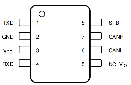 Figure 4-1 SOIC (D) Pin
Diagram
 Figure 4-3 SOT (DDF) Pin
Diagram
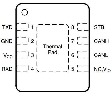 Figure 4-2 VSON
(DRB) Pin
Diagram
Figure 4-2 VSON
(DRB) Pin
DiagramFollowing are the assumptions of use
and the device configuration assumed for the pin FMA in this section:
- VCC = 4.5V to 5.5V
- VBAT = 6V to 24V
- VIO = 1.7V to 5.5V
Table 4-2 Pin FMA for Device Pins
Short-Circuited to Ground| Pin Name | Pin No. | Description of Potential Failure Effects | Failure Effect Class |
|---|
| TXD | 1 | Device enters dominant time out mode. Unable to transmit
data. | B |
| GND | 2 | None. | D |
| VCC | 3 | Device not powered, high ICC current. | B |
| RXD | 4 | RXD default is high-side FET ON, with pin short to ground, RXD forms
direct path between supply and ground causing high current. | A |
| NC | 5 | None. | D |
| VIO | 5 | Device is in protected mode. Transceiver is passive on bus. | B |
| CANL | 6 | VO(REC) specification violated. Degraded EMC
performance. | C |
| CANH | 7 | Device cannot drive dominant to the bus, no communication is
possible. | B |
| STB | 8 | STB stuck low, transceiver unable to
enter low-power mode. | B |
| Thermal Pad | - | None. | D |
Note: The VSON
(DRB)
package includes a thermal pad.
Table 4-3 Pin FMA for Device Pins
Open-Circuited| Pin Name | Pin No. | Description of Potential Failure Effects | Failure Effect Class |
|---|
| TXD | 1 | TXD pin defaults high, device always
recessive and unable to transmit data. | B |
| GND | 2 | Device not powered. | B |
| VCC | 3 | Device not powered. | B |
| RXD | 4 | No RXD output, unable to receive
data. | B |
| NC | 5 | None. | D |
| VIO | 5 | Device is in protected mode. Transceiver passive on bus. | B |
| CANL | 6 | Device cannot drive dominant on the bus,
unable to communicate. | B |
| CANH | 7 | Device cannot drive dominant on the bus,
unable to communicate. | B |
| STB | 8 | STB pin defaults high, transceiver stuck
in low-power mode. | B |
| Thermal Pad | - | None. | D |
Note: The VSON
(DRB)
package includes a thermal pad.
Table 4-4 Pin FMA for Device Pins
Short-Circuited to Adjacent Pin| Pin Name | Pin No. | Shorted to | Description of Potential Failure Effects | Failure Effect Class |
|---|
| TXD | 1 | GND | Device enters dominant time out mode. Unable to transmit
data. | B |
| GND | 2 | VCC | Device not powered, high ICCcurrent. | B |
| VCC | 3 | RXD | RXD output stuck high, unable to receive
data. | B |
| NC | 5 | CANL | None. | D |
| VIO | 5 | CANL | Bus stuck recessive, no communication is possible. IOS
current can be reached on CANL. | B |
| CANL | 6 | CANH | Bus stuck recessive, no communication is possible. IOS
current can be reached on CANH/CANL. | B |
| CANH | 7 | STB | Driver and receiver turn off when a dominant is driven. Not being
able to enter normal mode is possible. | B |
Note: The VSON
(DRB)
package includes a thermal pad. All device pins are adjacent to the thermal pad. The
device behavior when pins are shorted to the thermal pad depends on which net is
connected to the thermal pad.
Table 4-5 Pin FMA for Device Pins Short-Circuited to
VCC| Pin Name | Pin No. | Description of Potential Failure Effects | Failure Effect Class |
|---|
| TXD | 1 | TXD stuck high, unable to transmit
data. | B |
| GND | 2 | Device not powered, high ICC current. | B |
| VCC | 3 | None. | D |
| RXD | 4 | RXD pin stuck high, unable to receive data. | B |
| NC | 5 | None. | D |
| VIO | 5 | IO pins operate as 5V input and outputs. Microcontroller can be
damaged if VCC > VIO. | C |
| CANL | 6 | RXD always recessive, no communication is possible. IOS
current can be reached. | B |
| CANH | 7 | VO(REC) specification violated, degraded EMC
performance. | C |
| STB | 8 | STB stuck high, transceiver always in
standby mode. | B |
Table 4-6 Pin FMA for Device Pins Short-Circuited to VBAT| Pin Name | Pin No. | Description of Potential Failure Effects | Failure Effect Class |
|---|
| TXD | 1 | Absolute maximum violation, transceiver can be damaged. Unable to
transmit data. | A |
| GND | 2 | Device not powered, high IBAT current | B |
| VCC | 3 | Absolute maximum violation, transceiver can be damaged. Bus can be
unable to communicate. | A |
| RXD | 4 | Absolute maximum violation, transceiver can be damaged. Unable to
receive data. | A |
| NC | 5 | None. | D |
| VIO | 5 | Absolute maximum violation, transceiver can be damaged. | A |
| CANL | 6 | RXD always recessive, no communication is possible. IOS
current can be reached. | B |
| CANH | 7 | VO(REC) specification violated, degraded EMC
performance. | C |
| STB | 8 | Absolute maximum violation, transceiver can be damaged. Transceiver
stuck in low-power mode. | A |
Table 4-7 Pin FMA for Device Pins Short-Circuited to
VIO| Pin Name | Pin No. | Description of Potential Failure Effects | Failure Effect Class |
|---|
| TXD | 1 | TXD stuck high, unable to transmit
data. | B |
| GND | 2 | Device not powered, high IIO current. | B |
| VCC | 3 | IO pins operate as 5V input and outputs. Microcontroller can be
damaged if VCC > VIO. | C |
| RXD | 4 | RXD pin stuck high, unable to receive
data. | B |
| NC | 5 | None. | D |
| VIO | 5 | None. | D |
| CANL | 6 | RXD always recessive, no communication is possible. IOS
current can be reached is VIO ≥ 3.3V. | B |
| CANH | 7 | VO(REC) specification violated if VIO ≥ 3.3V,
degraded EMC performance. | C |
| STB | 8 | STB stuck high, transceiver always in
standby mode. | B |
Note: Table 4-7 is only applicable to the
TCAN844-Q1 and
TCAN844V-Q1
device.
 Figure 4-1 SOIC (D) Pin
Diagram
 Figure 4-3 SOT (DDF) Pin
Diagram
 Figure 4-2 VSON
(DRB) Pin
Diagram