SLAA654A November 2014 – July 2015 CC430F6147 , MSP430F412 , MSP430F413 , MSP430F4132 , MSP430F415 , MSP430F4152 , MSP430F417 , MSP430F423A , MSP430F4250 , MSP430F425A , MSP430F4260 , MSP430F4270 , MSP430F427A , MSP430F435 , MSP430F4351 , MSP430F436 , MSP430F4361 , MSP430F437 , MSP430F4371 , MSP430F438 , MSP430F439 , MSP430F447 , MSP430F448 , MSP430F4481 , MSP430F449 , MSP430F4491 , MSP430F4616 , MSP430F46161 , MSP430F4617 , MSP430F46171 , MSP430F4618 , MSP430F46181 , MSP430F4619 , MSP430F46191 , MSP430F47126 , MSP430F47127 , MSP430F47163 , MSP430F47166 , MSP430F47167 , MSP430F47173 , MSP430F47176 , MSP430F47177 , MSP430F47183 , MSP430F47186 , MSP430F47187 , MSP430F47193 , MSP430F47196 , MSP430F47197 , MSP430F477 , MSP430F478 , MSP430F4783 , MSP430F4784 , MSP430F479 , MSP430F4793 , MSP430F4794 , MSP430F6433 , MSP430F6435 , MSP430F6436 , MSP430F6438 , MSP430F6458 , MSP430F6459 , MSP430F6630 , MSP430F6631 , MSP430F6632 , MSP430F6633 , MSP430F6634 , MSP430F6635 , MSP430F6636 , MSP430F6637 , MSP430F6638 , MSP430F6658 , MSP430F6659 , MSP430F6720 , MSP430F6720A , MSP430F6721 , MSP430F6721A , MSP430F6723 , MSP430F6723A , MSP430F6724 , MSP430F6724A , MSP430F6725 , MSP430F6725A , MSP430F6726 , MSP430F6726A , MSP430F6730 , MSP430F6730A , MSP430F6731 , MSP430F6731A , MSP430F6733 , MSP430F6733A , MSP430F6734 , MSP430F6734A , MSP430F6735 , MSP430F6735A , MSP430F6736 , MSP430F6736A , MSP430F6745 , MSP430F67451 , MSP430F67451A , MSP430F6745A , MSP430F6746 , MSP430F67461 , MSP430F67461A , MSP430F6746A , MSP430F6747 , MSP430F67471 , MSP430F67471A , MSP430F6747A , MSP430F6748 , MSP430F67481 , MSP430F67481A , MSP430F6748A , MSP430F6749 , MSP430F67491 , MSP430F67491A , MSP430F6749A , MSP430F67621 , MSP430F67621A , MSP430F67641 , MSP430F67641A , MSP430F6765 , MSP430F67651 , MSP430F67651A , MSP430F6765A , MSP430F6766 , MSP430F67661 , MSP430F67661A , MSP430F6766A , MSP430F6767 , MSP430F67671 , MSP430F67671A , MSP430F6767A , MSP430F6768 , MSP430F67681 , MSP430F67681A , MSP430F6768A , MSP430F6769 , MSP430F67691 , MSP430F67691A , MSP430F6769A , MSP430F6775 , MSP430F67751 , MSP430F67751A , MSP430F6775A , MSP430F6776 , MSP430F67761 , MSP430F67761A , MSP430F6776A , MSP430F6777 , MSP430F67771 , MSP430F67771A , MSP430F6777A , MSP430F6778 , MSP430F67781 , MSP430F67781A , MSP430F6778A , MSP430F6779 , MSP430F67791 , MSP430F67791A , MSP430F6779A , MSP430FE423 , MSP430FE4232 , MSP430FE423A , MSP430FE4242 , MSP430FE425 , MSP430FE4252 , MSP430FE425A , MSP430FE427 , MSP430FE4272 , MSP430FE427A , MSP430FG4250 , MSP430FG4260 , MSP430FG4270 , MSP430FG437 , MSP430FG438 , MSP430FG439 , MSP430FG4616 , MSP430FG4617 , MSP430FG4618 , MSP430FG4619 , MSP430FG477 , MSP430FG478 , MSP430FG479 , MSP430FG6425 , MSP430FG6426 , MSP430FG6625 , MSP430FG6626 , MSP430FR4131 , MSP430FR4132 , MSP430FR4133 , MSP430FR5870 , MSP430FR5872 , MSP430FR58721 , MSP430FR5922 , MSP430FR59221 , MSP430FR5970 , MSP430FR5972 , MSP430FR59721 , MSP430FR6820 , MSP430FR6822 , MSP430FR68221 , MSP430FR6870 , MSP430FR6872 , MSP430FR68721 , MSP430FR6877 , MSP430FR6879 , MSP430FR68791 , MSP430FR6887 , MSP430FR6888 , MSP430FR6889 , MSP430FR68891 , MSP430FR6920 , MSP430FR6922 , MSP430FR69221 , MSP430FR6927 , MSP430FR69271 , MSP430FR6928 , MSP430FR6970 , MSP430FR6972 , MSP430FR69721 , MSP430FR6977 , MSP430FR6979 , MSP430FR69791 , MSP430FR6987 , MSP430FR6988 , MSP430FR6989 , MSP430FR69891 , MSP430FW423 , MSP430FW425 , MSP430FW427 , MSP430FW428 , MSP430FW429
- Designing With MSP430™ MCUs and Segment LCDs
- Revision History
4.3 Biasing
The highest voltage level V1 is generated by VLCD. VLCD can be sourced either externally, or from the internal charge pump as discussed in Section 4.2. To produce the rest of the voltage levels in the LCD waveforms, V2 through V5, the module needs to be able to produce bias voltages at fractions of VLCD.
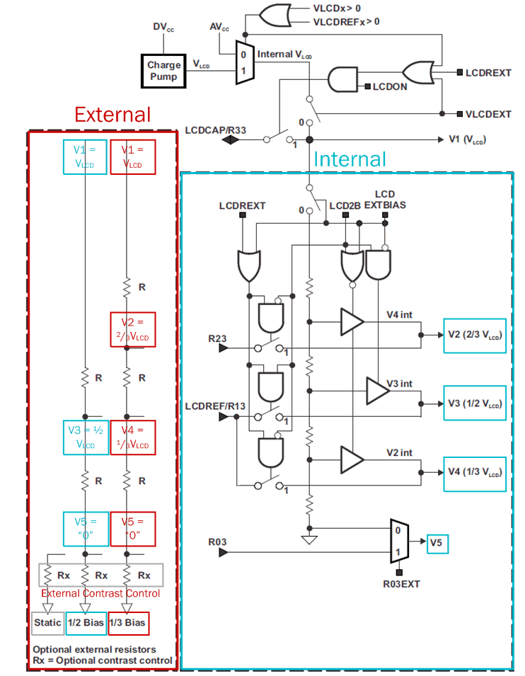
The bias voltages V2 through V5 can be divided down from VLCD either internally or with an external resistor network. This selection is entirely independent of how VLCD is being sourced (there can be any combination of internal/external VLCD source, and internal/external bias voltage generation). Depending on the muxing being used and the specific MSP430 device, different bias options like 1/2 or 1/3 may be available – check the device specific data sheet and user's guide. For 1/2 bias mode, voltage levels V1, V3, and V5 are used in the waveforms – V1 = VLCD, V3 = 1/2 VLCD, and V5 = 0. For 1/3 bias mode, voltage levels V1, V2, V4, and V5 are used in the waveforms – V1 = VLCD, V2 = 2/3 VLCD, V4 = 1/3 VLCD, and V5 = 0. Figure 6 shows an example of the possible internal and external bias options in one of the LCD modules.
Generating bias voltages internally is simple because no external components are required – the module internally divides down the voltage. However, generating bias voltages externally instead can be lower power. External biasing requires the user to provide an external resistor divider to create the voltages V2 through V5 - the resistor divider used depends on the biasing mode – static, 1/2, or 1/3 bias as you can see in Figure 6. The resistors in the divider should all be the same value, but the size used may depend on the particular display used in the design.
Changing the external resistor values can impact both current consumption and contrast – see the application note Driving Large LCD With LCD Peripheral of the MSP430 (SLAA272) for more details on these tradeoffs and selecting the size of the resistors for the divider. Larger resistors cause less current consumption in the resistor ladder, saving you power – however, if resistors are too large, the contrast may not be good or may not be even for all segments. Experimentation with different sizes of resistor is usually needed in a design to find the best combination of performance vs current consumption.
 Figure 6. Bias Configurations