SLAA842B December 2018 – August 2019 DS90C401 , DS90C402 , MSP430FR2512 , MSP430FR2522 , MSP430FR2532 , MSP430FR2533 , MSP430FR2632 , MSP430FR2633 , MSP430FR2672 , MSP430FR2673 , MSP430FR2675 , MSP430FR2676
6 Step 4: Hardware Development
The fourth step of designing a successful capacitive touch sensing system is to develop the hardware for the application. This section provides the hardware development guidance for CapTIvate MCUs.
Step 4a: Schematic Design Checklist
Table 10. Schematic Design Checklist
| No. | Components | Recommendations |
|---|---|---|
| 1 | VREG pin decoupling capacitor | 1 µF, low ESR ≤200 mΩ, placed next to VREG pin |
| 2 | DVCC pin decoupling capacitor | 4.7-µF to 10-µF tank, 0.1-µF bypass, placed next to MCU |
| 3 | Series resistors on CAP I/Os | 470 Ω |
| 4 | EMI noise filter capacitor | 68 pF, required for mutual capacitance mode RX pins if require conducted noise immunity |
| 5 | Reset pin resistor and capacitor | 47-kΩ pullup with 1-nF pulldown |
| 6 | I2C communication lines pullup resistor | 2.2 kΩ |
| 7 | Bootloader (BSL) | Refer to the bootloader section of the device-specific data sheet for BSL pin requirement and functions. |
| 8 | CAP I/O pins assignment (if possible) |
Use CapTIvate Design Center to auto-assign the CAP I/O pins. Leverage all the CapTIvate blocks. Use dedicated CAP I/O pins first. Refer to CapTIvate Pin Selection Guide. |
Step 4a.1: VREG Pin Decoupling Capacitor
VREG is the decoupling capacitor of the CapTIvate regulator. The recommended value for the required decoupling capacitor is 1 µF, with a maximum ESR of ≤200 mΩ. Connect VREG as close as possible to the MCU.
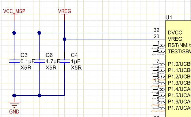 Figure 3. VREG Pin Decoupling Capacitor
 Step 4a.2: DVCC Pin Decoupling Capacitor
Refer to the device-specific data sheet for details.
Step 4a.3: Series Resistors on CAP I/Os
These are multipurpose series resistors that work with a TPD1E10B06 transient-voltage suppressor (TVS) diode if the system requires Electrostatic Discharge (ESD) protection. These resistors also help to lower the system emissions and improve RF noise immunity.
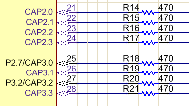 Figure 4. Series Resistors on CAP I/Os
 Step 4a.4: EMI Noise Filter Capacitor
For conducted noise immunity considerations, add a 68-pF capacitor to only mutual capacitance mode RX pins. The additional capacitance helps to minimize the effects of EMI. If DVCC mode is enabled, this capacitor can also help to ensure that the ratio of RX parasitic capacitance (Cp) to RX-TX mutual capacitance (Cm) is within the range that is specified in the data sheet.
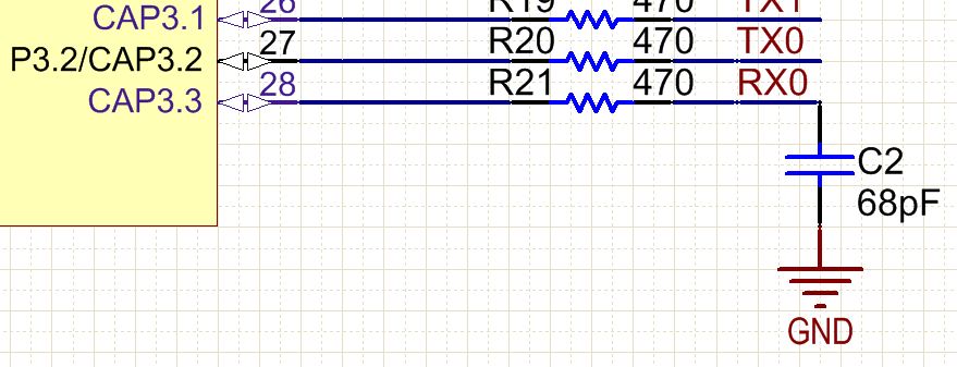 Figure 5. EMI Noise Filter Capacitor
 Step 4a.5: Reset Pin Resistor and Capacitor
Refer to the device-specific data sheet for details.
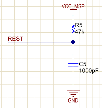 Figure 6. Reset Pin Resistor and Capacitor
 Step 4a.6: I2C Communication Lines Pullup Resistor
Refer to the device-specific data sheet for details.
Step 4a.7: Bootloader (BSL)
Refer to the device-specific data sheet and the MSP430 FRAM Device Bootloader (BSL) User's Guide for details.
Step 4a.8: CAP I/O Pin Assignments
Every CAP I/O pin can be configured as a self capacitance or mutual capacitance sensor. To leverage the parallel scanning feature that reduces the overall power consumption and increases the response rate, you must optimize the CAP I/O pins assignment. CapTIvate Design Center has an auto-assign feature to optimize the CAP I/O pins assignment before schematic design. You can also use CapTIvate Design Center to evaluate an existing pin assignment and attempt to reduce the number of scan cycles. Figure 7 shows the auto-assign feature optimize 12 buttons with only 3 time cycles.
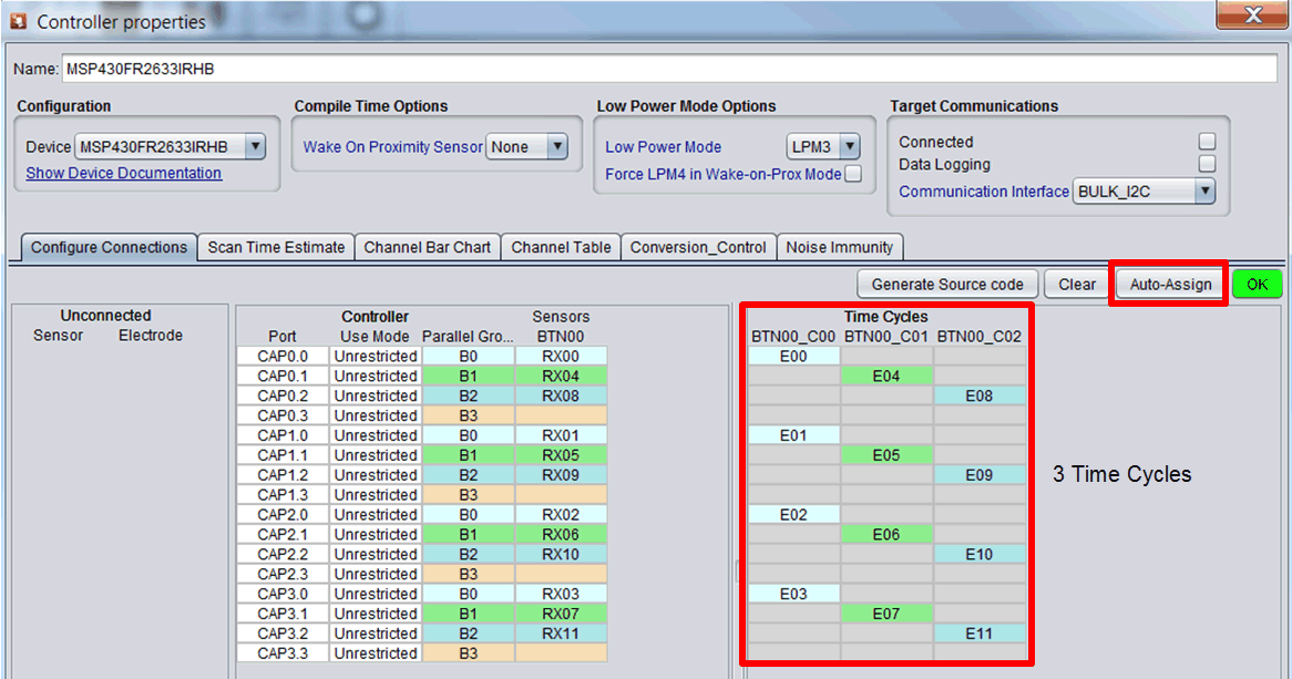 Figure 7. Auto-Assign Feature
 Try to use all of the available CapTIvate blocks to enable parallel scanning. The number of CapTIvate measurement blocks on a device determines the number of sensing electrodes that can be measured simultaneously. For example, if a device has 4 blocks and 6 buttons in a design, Figure 8 shows two different pin assignment and the required scan cycles.
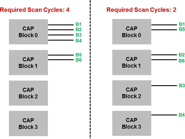 Figure 8. Scan Time Cycles
 If the device supports dedicated CAP I/O pins, assign the sensors to those CAP I/Os first. This can save the GPIOs for other uses in the application.
Refer to the CapTIvate Pin Selection section of the CapTIvate™ Technology Guide for details.
Step 4b: PCB Layout Design Checklist
Table 11. PCB Layout Design Checklist
| No. | Components | Recommendations | |
|---|---|---|---|
| 1 | Buttons (self capacitance) | Size | 10 mm and 12 mm (side length of square button, diameter of round button), equivalent to the interaction area |
| Shape | Various, typically round or square | ||
| Spacing to surrounding | 0.5 × overlay minimum thickness | ||
| 2 | Buttons (mutual capacitance) | Size | 10 mm and 12 mm (side length of square button, diameter of round button), equivalent to the interaction area |
| Shape | Various, recommend square or shape with corners | ||
| RX thickness | 0.5 mm (typical) | ||
| TX thickness | 1 mm (typical) | ||
| RX-to-TX spacing | 0.5 mm (typical) | ||
| 3 | Sliders and wheels | Shape | Sliders: Linear shape. Wheels: Circular shape.
Refer to Automating Capacitive Touch Slider and Wheel PCB Design Using OpenSCAD Scripts. |
| Size | Depends on the required touch area | ||
| Number of electrodes | 3 or 4 electrodes | ||
| 4 | Proximity | Varies from design to design | |
| 5 | Sensor trace | Width | 8 mil or as thin as the PCB manufacture allows |
| Length | Minimize the length from sensor to controller | ||
| 6 | LEDs | LEDs signals 4 mm away from sensor signals | |
| 7 | Ground pour | Use hatched pour instead of solid pour.
Hatching: 25% (typical) 45°, 8-mil track width, 64-mil grid size |
|
| 8 | Moisture and liquid | Refer to Moisture Design Consideration and the Liquid Tolerant Capacitive Touch Keypad reference design | |
| 9 | Metal touch | Refer to Capacitive Touch Through Metal Using MSP430™ MCUs With CapTIvate™ Technology | |
| 10 | Noise immunity | Refer to Noise Immunity Hardware for details. | |
Step 4b.1: Buttons, Self Capacitance
- A self capacitive button sensor is a single electrode. Self capacitive buttons are simple to layout and each button is assigned to only one pin on the MCU.
- Button size ranges from 6 mm to 15 mm (side length of square button, diameter of round button) and depends on the required touch area.
- The typical shape for a self-capacitance button is rectangular or round.
Refer to Self Capacitance Buttons Design and Electrode Size and Overlay Thickness for details.
 Figure 9. Button Shape for Self Capacitance
 Step 4b.2: Buttons, Mutual Capacitance
- A mutual capacitance button sensor requires two electrodes, one as a TX and the other for RX. TX on outside and RX on inside.
- Button size ranges from 6 mm to 15 mm (side length of square button, diameter of round button), depending on the required touch area.
- Figure 11 shows an optimized layout for selecting TX and RX pins in an application with 12 mutual-capacitance buttons. This layout is optimized to reduce the number of pins and scan cycles.
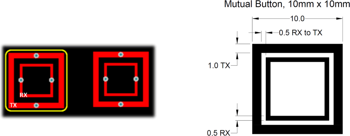 Figure 10. Button Shape for Mutual Capacitance
 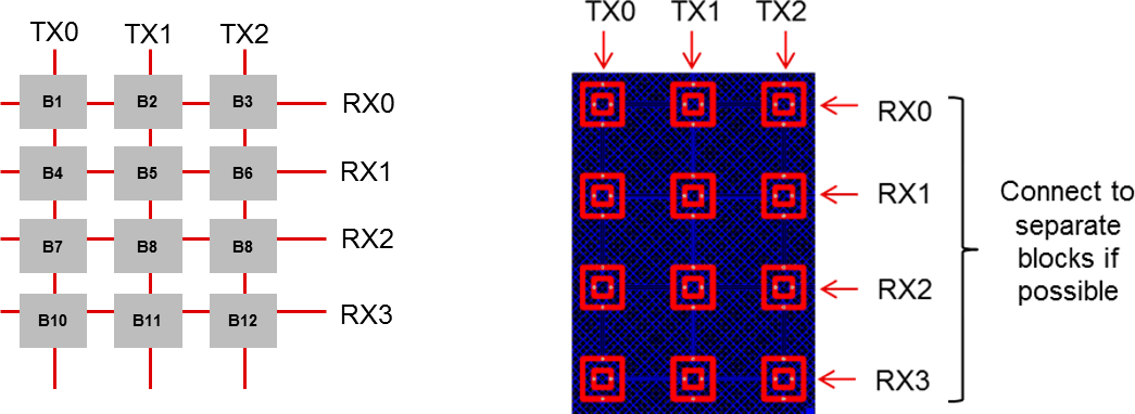 Figure 11. Mutual-Capacitance Matrix
 Refer to Mutual Capacitance Buttons Design and Electrode Size and Overlay Thickness for details.
Step 4b.3: Sliders and Wheels
- Sliders and wheels have the best performance when they have well-balanced sensitivities across all electrodes.
- The area of the electrode is not as critical as the percentage of coverage across multiple electrodes. Interdigitated slider and wheel designs provide the most efficient and optimal coupling but can be complicated to create. Simpler designs are possible but require experimentation.
- Self capacitance slider and wheel
- Mutual capacitance slider and wheel
 Figure 12. Self Capacitive Slider and Wheel
  Figure 13. Mutual Capacitive Slider and Wheel
 Refer to Slider and Wheels Design and Implement custom slider/wheel position algorithm for details.
Step 4b.4: Proximity
The sensing range of a proximity sensor is dependent upon several factors:
- The size and shape of the proximity sensor
- The sensor configuration tuning values
- The surrounding conductors
- The system surrounding environment
Refer to Proximity Sensing Design for details.
Step 4b.5: Sensor Traces
- Keep the width of the sensor traces less than 8 mil or as thin as the PCB manufacture allows
- Minimize the length of the sensor trace from the sensor electrodes to controller
- Do not have 90° turns, because the sharp turns can pick up noise.
- Sensor traces routing considerations:
- Try to route the sensor trace on the bottom layer of the PCB so the user will not interact with the sensor traces.
- Do not run digital signals like PWM signals or communications line like I2C or SPI near the sensor trace. It is recommended to keep these types of signals at least 4 mm away from the sensor trace. If the digital signal and the capacitive touch trace must cross, then it is recommended to keep the crossing at a 90 degree angle.
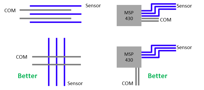 Figure 14. Sensor Traces Routing
 - Mutual capacitance routing considerations:
- Avoid routing TX lines near RX lines when possible. If unable to avoid routing TX and RX on the same layer, put a ground trace between TX and RX. If TX needs to cross RX, route the traces to that they cross perpendicular to each other.
- Route TX lines next to other TX lines. Route RX lines next to other RX lines.
- Keep grounds away from the TX and RX traces by half of the panel thickness.
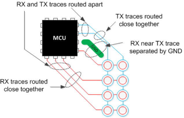 Figure 15. Mutual-Capacitance Routing Considerations
 Step 4b.6: LEDs
Signals that drive LEDs (unless the LEDs require high-strength drivers) are similar to other digital signals. As with digital signals, avoid placing LEDs signals near the sensor trace. TI recommends a distance of at least 4 mm for SLED (see Figure 16).
 Figure 16. LED Routing
 Refer to LEDs/LED Backlighting for details.
Step 4b.7: Ground Pour
- When adding a ground pour near a sensor electrode, there is a tradeoff between maintaining high sensor sensitivity and increasing the noise immunity of the system.
- The use of a hatched pour instead of a solid ground pour is a good design practice. A hatched pour reduces the parasitic capacitance from the ground pour. Typically, a 25% fill hatch is sufficient, but this percentage can be increased or decreased to improve noise immunity or sensitivity, respectively.
- When designing a button, slider, or wheel of any size or shape, a flexible method to control the distance between any sensor and the ground pour is to provide a poly cut-out region around the sensor (see Figure 17). The gap from the sensors to the surrounding ground can be 0.5 mm to 2 mm and is typically equal to half of the overlay thickness.
 Figure 17. Ground Pour
 Refer to Ground Planes for details.
Step 4b.8: Moisture and Liquid
- Moisture and liquid rejection: The system is designed to block sensor detection if moisture or liquid is detected. Refer to Moisture Design Consideration.
- Moisture and liquid tolerant: The system is designed to work properly when exposed to moisture or liquid with limitations on the sensor spacing and the orientation of the sensor placing. Refer to the Liquid Tolerant Capacitive Touch Keypad Reference Design.
Step 4c: Mechanical Design
Table 12 is a mechanical design checklist.
Table 12. Mechanical Design Checklist
| No. | Components | Recommendations | |
|---|---|---|---|
| 1 | Overlay | Material | Typical: glass, polycarbonate, acrylic, ABS. Avoid conductive materials and conductive paints. |
| Thickness | 10 mm or thinner, depends on material and sensor size | ||
| Stackup |
Self capacitance: Avoid an air gap Mutual capacitance: Cannot have an air gap Can use materials to bridge the gap like spring clips. |
||
| Bounding | Typical: optically clear adhesive, screws | ||
| 2 | Enclosure | Varies from design to design | |
| 3 | Connector | Minimize the trace length from the sensor to the MCU. Make sure that the connector is mechanically stable during operation. | |
| 4 | Sensor material | Typical: PCB, FPC, copper tape, conductive wire, ITO | |
| 5 | Noise immunity | Refer to Noise Immunity Hardware. | |
| 6 | Metal touch | Refer to the metal touch application design guide, Capacitive Touch Through Metal. | |
Step 4c.1: Overlay
Material and Thickness
- The overlay material's dielectric constant (εr) and thickness play an important role in determining the strength of the electric field at the surface of the sensor.
- The dielectric constant determines how efficiently electric field propagates through material and the distance between the overlay and the sensor determines how much electric field reaches the target contact area. For example, if all other factors are the same, a 5-mm overlay with εr of 4 has similar sensitivity to a 2.5-mm overlay with εr of 2.
- Conductive materials interfere with the electric field. We recommend to not using conductive materials for overlay including the conductive paints.
Stackup and Bounding
- Make sure that there is good contact between the overlay and the sensor electrode to ensure good sensitivity and reliable performance. Always avoid air gaps between the sensor electrode and overlay, especially in a mutual capacitive design. If the mechanical stackup requires a gap, use a filler material. Pressure sensitive adhesive tape can fill a narrow gap, and mechanical springs can fill a wide gap.
- The most common bounding method is using nonconductive optically clear adhesive film and this can increase the sensitivity by eliminating the air gap. Typical adhesive used are 3M™ 200MP, 467MP and 468MP.
No air gap is allowed in a mutual capacitive design.
Refer to Overlay Design and Gaps Consideration for details.
Step 4c.2: Enclosure
The choice of enclosure depends on the product industrial design and also the requirement for the capacitive touch subsystem. For example, in moisture tolerant capacitive touch design you should use a non-conductive enclosure if possible. However, metallic enclosure that can be tied to a ground is better for ESD discharge.
Step 4c.3: Connector
- Do not use a connector between the sensor and the MCU if possible, because a parasitic capacitance is associated with the connector PCB footprint and structure.
- If possible, place the MCU on the touch sensor PCB and route power and communication lines through the connector to the main PCB.
- Flex PCB or FPC can be used as an interconnection between PCBs, but make sure that it is mechanically stable during product operation.
Refer to Connector Consideration for details.
Step 4c.4: Sensor Materials
- Common sensor electrode materials include PCB, FPC, copper tape, conductive wire, and ITO.
- When using copper tape or conductive wire for the sensor electrode, do not run them in close proximity to a metal enclosure or other noise signals in the system.
Refer to Electrode and Trace Materials for details.