SLAAE46 November 2021 DAC43701
2 NVM Online Update to Minimize Flicker
After the VDD supply has been established, and before the communication between the MCU and DAC43701 is valid, the default state of DAC_OUT is powered down to high impedance. During this time,the VCOM will be . If this duration is too long, it will cause a visible flicker at the LCD panel. When the system powers up, VCOM should be set to 0V as soon as possible to minimize flicker. Therefore, the DAC_OUT default state should be modified, which can be done by updating the NVM of the DAC43701.
A common method of programming the NVM is by monolithic flash in the factory. This method can require additional customized tools and mass production procedures. In addition, if the DAC43701 needs to be replaced, the new device will need to be reprogrammed which can be an inconvenience for subsequent maintenance. If the application uses an MCU or other I2C masters, there is a simpler method available to program the NVM. This method to update the NVM with the LCD system’s existing MCU (NVM online update) is described below.
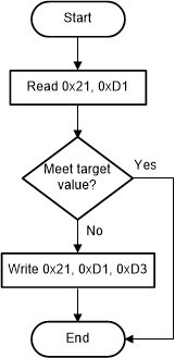
As shown in Equation 3 the DAC_DATA register should be set to to set VCOM to 0V. And the DAC_PDN bits in the GENERAL_CONFIG register (address = D1h) should be 00b to enable the DAC output. Figure 2-1 shows the flow of the NVM online update.
- After each POR delay, read back register 0x21 and 0xD1.
- Compare the read back values with the target values. Execute steps 3-5 if the values DO NOT meet the above target values.
- Update DAC_DATA(address = 21h) to customized value.
- Write 00b to DAC_PDN (address = D1h) to power up the DAC output.
- Assert NVM_PROG (address = D3h) to initiate NVM write.
- After programing and a power cycle, the DAC_OUT will have the target default state.
 Figure 2-1 Work Flow of the NVM Online Update
With the above flow, the MCU will automatically update the NVM in situations where there is a deviation from the target value such as replacing the DAC43701 with a new device, or an unsuccessful initialization caused by noise.
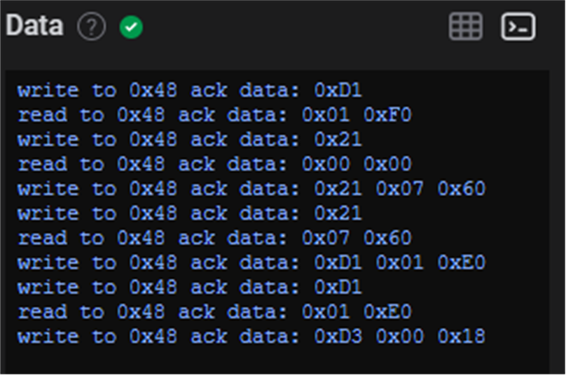
The following shows a pseudo code example of Figure 2-1 to program the initial register values to the NVM. The users can modify it for their dedicated usages. Figure 2-2 gives the I2C log when the target value of DAC_DATA (address = 21h) is 0x0760, and GENERAL_CONFIG (address = D1h) is 0x01E0.
Pseudo Code Example for NVM Online Update
//SYNTAX:WRITE <REGISTER NAME (REGISTER ADDRESS)>, <MSB DATA>, <LSB DATA>
//SYNTAX:READ <REGISTER NAME (REGISTER ADDRESS)>, <MSB DATA>, <LSB DATA>
READ DAC_DATA(0x21)
READ GENERAL_CONFIG (0xD1)
//Whether ‘target value’ or not
IF(0xD1=01E0h & 0x21= )
{}
ELSE
{
//Write DAC code (12-bit aligned)
WRITE DAC_DATA(0x21),
//Enable output, DAC_PDN=00,
WRITE GENERAL_CONFIG (0xD1), 0x01, 0xE0
//Program the NVM
WRITE TRIGGER(0xD3), 0x00, 0x18
//DAC output will go to target voltage at power up, and will have target output voltage next POR.
}
 Figure 2-2 I2C Log of the Work Flow