SLAT161 June   2022 HD3SS3411 , TMUXHS4412


  1.   Abstract
  2.   Trademarks
  3. 1Introduction
  4. 2What is PCI Express (PCIe)?
    1. 2.1 PCIe Link
    2. 2.2 PCIe Clocking Architectures
      1. 2.2.1 Common Reference Clock
      2. 2.2.2 Data Reference Clock
      3. 2.2.3 Separate Reference Clock
    3. 2.3 PCIe Reference Clock Specification
  5. 3Reference Clock Measurement With TI Multiplexers
    1. 3.1 Test Setup and Procedure
      1. 3.1.1 Test Setup
      2. 3.1.2 Test Procedure
    2. 3.2 Test Report
      1. 3.2.1 Test Result With Clock Source
      2. 3.2.2 Test Result With HD3SS3411
      3. 3.2.3 Test Result With TMUXHS4412
      4. 3.2.4 Test Result With TMUXHS221
  6. 4Summary

Separate Reference Clock

Another clocking architecture is the Separate Reference architecture where a different clock source is used at each end of the PCIe link. The advantage of this architecture is that tightly controlled reference clock distribution is no longer required over connectors and backplanes.
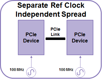
GUID-20220628-SS0I-6TDZ-FXJG-WJ7HTMP27HL4-low.png Figure 2-4 Seperate Clock Architecture

From three refclk architecture, the common refclk architecture is the easiest and most commonly used method for clock distribution among PCIe devices. Only test common refclk architecture is tested in this application report.