SLAU298A November 2009 – May 2021
- Trademarks
- 1ADS8555EVM-PDK Overview
- 2EVM Analog Interface
- 3Digital Interface
- 4Power Supplies
- 5Installing the ADS8555EVM Software
-
6ADS8555EVM Operation
- 6.1 Connecting the Hardware and Running the GUI
- 6.2 Jumper Settings for the ADS8555EVM
- 6.3 Modifying Hardware and Using Software to Evaluate Other Devices in the Family
- 6.4 EVM GUI Global Settings for ADC Control and Registers
- 6.5 Time Domain Display
- 6.6 Frequency Domain Display
- 6.7 Histogram Display
- 7Bill of Materials, Layout, and Schematics
- 8Revision History
6.7 Histogram Display
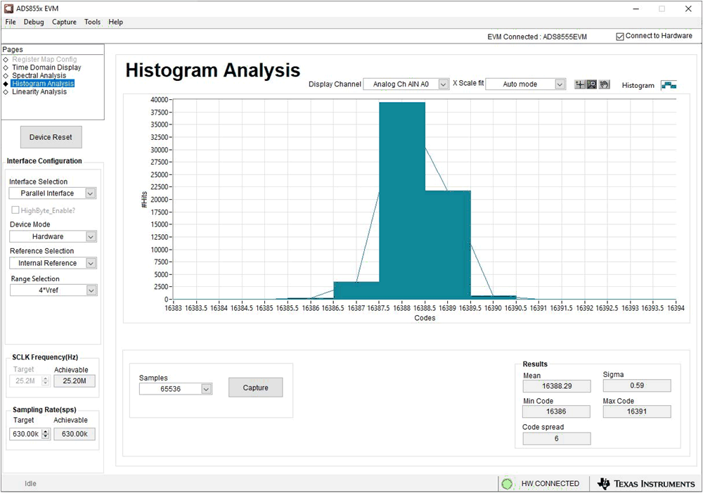
Noise degrades ADC resolution and the histogram tool can be used to estimate effective resolution, which is an indicator of the number of bits of ADC resolution losses resulting from noise generated by the various sources connected to the ADC when measuring a DC signal. The cumulative effect of noise coupling to the ADC output from sources such as the input drive circuits, the reference drive circuit, the ADC power supply, and the ADC itself is reflected in the standard deviation of the ADC output code histogram that is obtained by performing multiple conversions of a DC input applied to a given channel. As shown in Figure 6-8, the histogram corresponding to a DC input is displayed on clicking the Capture button.
 Figure 6-8 Histogram Display