SLAU298A November 2009 – May 2021
- Trademarks
- 1ADS8555EVM-PDK Overview
- 2EVM Analog Interface
- 3Digital Interface
- 4Power Supplies
- 5Installing the ADS8555EVM Software
-
6ADS8555EVM Operation
- 6.1 Connecting the Hardware and Running the GUI
- 6.2 Jumper Settings for the ADS8555EVM
- 6.3 Modifying Hardware and Using Software to Evaluate Other Devices in the Family
- 6.4 EVM GUI Global Settings for ADC Control and Registers
- 6.5 Time Domain Display
- 6.6 Frequency Domain Display
- 6.7 Histogram Display
- 7Bill of Materials, Layout, and Schematics
- 8Revision History
7.3 Schematics
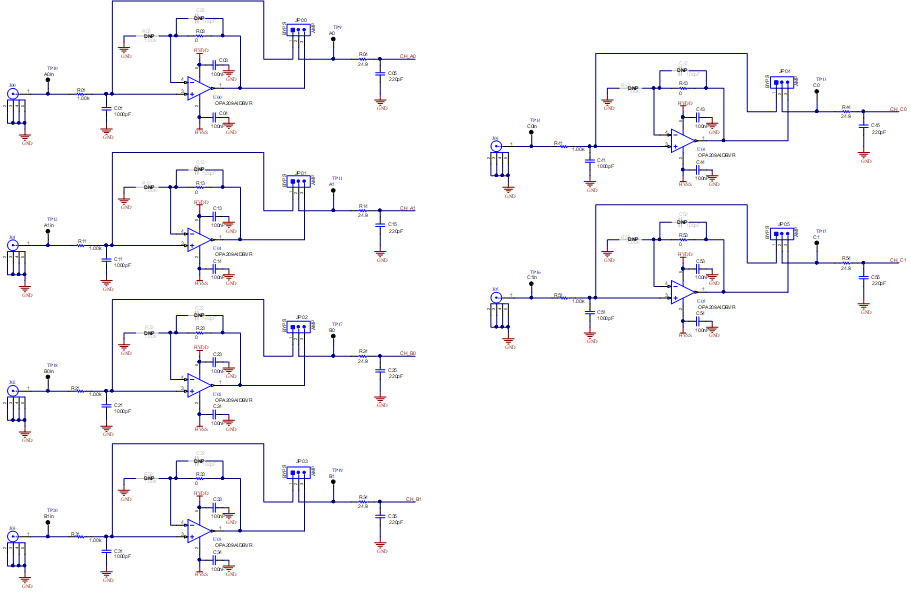
Figure 7-2 shows a schematic for the amplifier drive section of the ADS8555EVM. The amplifier is by default a buffer and can be bypassed by using a jumper.
 Figure 7-2 Amplifier Drive Schematic
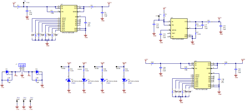
Figure 7-3 shows the LDOs used to generate the AVDD, HVDD, and HVSS supplies.
 Figure 7-3 LDO Schematic
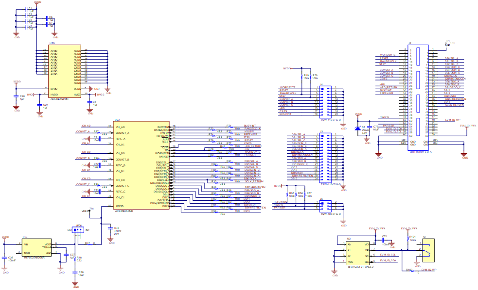
Figure 7-4 shows the ADC decoupling, digital connections, and reference connections.
 Figure 7-4 ADC, Reference, and Digital I/O
Schematic