SLAU298A November 2009 – May 2021
- Trademarks
- 1ADS8555EVM-PDK Overview
- 2EVM Analog Interface
- 3Digital Interface
- 4Power Supplies
- 5Installing the ADS8555EVM Software
-
6ADS8555EVM Operation
- 6.1 Connecting the Hardware and Running the GUI
- 6.2 Jumper Settings for the ADS8555EVM
- 6.3 Modifying Hardware and Using Software to Evaluate Other Devices in the Family
- 6.4 EVM GUI Global Settings for ADC Control and Registers
- 6.5 Time Domain Display
- 6.6 Frequency Domain Display
- 6.7 Histogram Display
- 7Bill of Materials, Layout, and Schematics
- 8Revision History
6.5 Time Domain Display
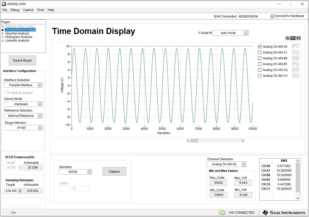
The time domain display tool allows visualization of the ADC response to a given input signal. This tool is useful for both studying the behavior and debugging any gross problems with the ADC or drive circuits. The user can trigger a capture of the data of the selected number of samples from the ADS8555EVM, as per the current interface mode settings indicated in Figure 6-6 by using the Capture button. The sample indices are on the x-axis and there are two y-axes showing the corresponding output codes as well as the equivalent analog voltages based on the specified reference voltage. Switching pages to any of the analysis tools described in the subsequent sections causes calculations to be performed on the same set of data.
 Figure 6-6 Time Domain Display