SLAU367P October 2012 – April 2020 MSP430FR5041 , MSP430FR5043 , MSP430FR50431 , MSP430FR5847 , MSP430FR58471 , MSP430FR5848 , MSP430FR5849 , MSP430FR5857 , MSP430FR5858 , MSP430FR5859 , MSP430FR5867 , MSP430FR58671 , MSP430FR5868 , MSP430FR5869 , MSP430FR5870 , MSP430FR5872 , MSP430FR58721 , MSP430FR5887 , MSP430FR5888 , MSP430FR5889 , MSP430FR58891 , MSP430FR5922 , MSP430FR59221 , MSP430FR5947 , MSP430FR59471 , MSP430FR5948 , MSP430FR5949 , MSP430FR5957 , MSP430FR5958 , MSP430FR5959 , MSP430FR5962 , MSP430FR5964 , MSP430FR5967 , MSP430FR5968 , MSP430FR5969 , MSP430FR5969-SP , MSP430FR59691 , MSP430FR5970 , MSP430FR5972 , MSP430FR59721 , MSP430FR5986 , MSP430FR5987 , MSP430FR5988 , MSP430FR5989 , MSP430FR5989-EP , MSP430FR59891 , MSP430FR5992 , MSP430FR5994 , MSP430FR59941 , MSP430FR6005 , MSP430FR6007 , MSP430FR6035 , MSP430FR6037 , MSP430FR60371 , MSP430FR6041 , MSP430FR6043 , MSP430FR60431 , MSP430FR6045 , MSP430FR6047 , MSP430FR60471 , MSP430FR6820 , MSP430FR6822 , MSP430FR68221 , MSP430FR6870 , MSP430FR6872 , MSP430FR68721 , MSP430FR6877 , MSP430FR6879 , MSP430FR68791 , MSP430FR6887 , MSP430FR6888 , MSP430FR6889 , MSP430FR68891 , MSP430FR6920 , MSP430FR6922 , MSP430FR69221 , MSP430FR6927 , MSP430FR69271 , MSP430FR6928 , MSP430FR6970 , MSP430FR6972 , MSP430FR69721 , MSP430FR6977 , MSP430FR6979 , MSP430FR69791 , MSP430FR6987 , MSP430FR6988 , MSP430FR6989 , MSP430FR69891
37.2.1.6 Comparator and DAC
The analog input signals are converted into digital signals by the comparator and the programmable 12-bit DAC. The comparator compares the selected analog signal to a reference voltage generated by the DAC. If the voltage is above the reference, the comparator output is high. Otherwise, it is low. The comparator outputs of both analog front-ends can be individually inverted by setting ESICA1INV for AFE1 or ESICA2INV for AFE2. The comparator output is stored in the selected output bit and processed by the processing state machine to detect motion and direction.
The comparator and the DAC in both analog front-ends AFE1 and AFE2 are turned on and off by ESICA(tsm) signal and the ESIDAC(tsm) signal. In case, the AFE1's comparator or DAC are not needed they can be disabled by clearing the ESICA(tsm) and ESIDAC(tsm) control bits within ESITSM0 register. AFE2 is disabled when its comparator and DAC are disabled. This can be done by clearing the ESICA2EN and ESIDAC2EN bits. In case these bits are set the AFE2's comparator and DAC will be controlled by the ESICA(tsm) and ESIDAC(tsm) control bits.
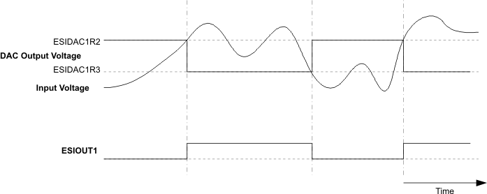
For each input there are two DAC registers to set the reference level as listed in Table 37-3. Together with the last stored output of the comparator, ESIOUTx, the two levels can be used as an analog hysteresis as shown in Figure 37-7. The individual settings for the four inputs can be used to compensate for mismatches between the sensors.
Table 37-3 Selected DAC Registers
| Analog Front-End | Selected Output Bit, ESIOUTx | Last Value of ESIOUTx | DAC Register Used |
|---|---|---|---|
| AFE1 | ESIOUT0 | 0 | ESIDAC1R0 |
| 1 | ESIDAC1R1 | ||
| ESIOUT1 | 0 | ESIDAC1R2 | |
| 1 | ESIDAC1R3 | ||
| ESIOUT2 | 0 | ESIDAC1R4 | |
| 1 | ESIDAC1R5 | ||
| ESIOUT3 | 0 | ESIDAC1R6 | |
| 1 | ESIDAC1R7 | ||
| AFE2 | ESIOUT4 | 0 | ESIDAC2R0 |
| 1 | ESIDAC2R1 | ||
| ESIOUT5 | 0 | ESIDAC2R2 | |
| 1 | ESIDAC2R3 | ||
| ESIOUT6 | 0 | ESIDAC2R4 | |
| 1 | ESIDAC2R5 | ||
| ESIOUT7 | 0 | ESIDAC2R6 | |
| 1 | ESIDAC2R7 |
 Figure 37-7 Analog Hysteresis With DAC Registers
 When TESTDX = 1, the ESIDAC1R6 and ESIDAC1R7 registers are used as the comparator reference as described in Table 37-4. Note that this feature is only available in AFE1.
Table 37-4 DAC Register Select When TESTDX=1
| ESITESTS1(tsm) | DAC Register Used |
|---|---|
| 0 | ESIDAC1R6 |
| 1 | ESIDAC1R7 |