SLAU723A October 2017 – October 2018 MSP432E401Y , MSP432E411Y
- 1
- 7
- 65
- 132
-
167
- 168
-
215
- 216
- 217
- 218
- 219
- 220
- 221
- 222
- 223
- 224
- 225
- 226
- 227
- 228
- 229
- 230
- 231
- 232
- 233
- 234
- 235
- 236
- 237
- 238
- 239
- 240
- 241
- 242
- 243
- 244
- 245
- 246
- 247
- 248
- 249
- 250
- 251
- 252
- 253
- 254
- 255
- 256
- 257
- 258
- 259
- 260
- 261
- 262
- 263
- 264
- 265
- 266
- 267
- 268
- 269
- 270
- 271
- 272
- 273
- 274
- 275
- 276
- 277
- 278
- 279
- 280
- 281
- 282
- 283
- 284
- 285
- 286
- 287
- 288
- 289
- 290
- 291
- 292
- 293
- 294
- 295
- 296
- 297
- 298
- 299
- 300
- 301
- 302
- 303
- 304
- 305
- 306
- 307
- 308
- 309
- 310
- 311
- 312
- 313
- 314
- 315
- 316
- 317
- 318
- 319
- 320
- 321
- 322
- 323
- 324
- 325
- 326
- 327
- 328
- 329
- 330
- 331
- 332
- 333
- 334
- 335
- 336
- 337
- 338
- 339
- 340
- 341
- 342
- 343
- 344
- 345
- 346
- 347
- 348
- 349
- 350
- 351
- 352
- 353
- 354
- 355
- 356
- 357
- 358
- 359
- 360
- 361
- 362
- 363
- 364
- 365
- 366
- 367
- 368
- 369
- 370
- 371
- 372
- 373
- 374
- 375
- 376
- 377
- 378
- 379
- 380
- 381
- 382
- 383
- 384
- 385
- 386
- 387
- 388
- 389
- 390
- 391
- 392
- 393
- 394
- 395
- 396
- 397
- 398
- 399
- 400
- 401
- 402
- 403
- 404
- 405
- 406
- 408
- 415
- 482
- 564
- 643
- 715
- 791
- 841
- 855
- 870
-
917
- 918
- 919
- 920
- 1002
- 1017
-
1021
- 1022
- 1023
- 1024
- 1025
- 1026
- 1027
- 1028
- 1029
- 1030
- 1031
- 1032
- 1033
- 1034
- 1035
- 1036
- 1037
- 1038
- 1039
- 1040
- 1041
- 1042
- 1043
- 1044
- 1045
- 1046
- 1047
- 1048
- 1049
- 1050
- 1051
- 1052
- 1053
- 1054
- 1055
- 1056
- 1057
- 1058
- 1059
- 1060
- 1061
- 1062
- 1063
- 1064
- 1065
- 1066
- 1067
- 1068
- 1069
- 1070
- 1071
- 1072
- 1073
- 1074
- 1075
- 1076
- 1077
- 1078
- 1079
- 1080
- 1081
- 1082
- 1083
- 1084
- 1085
- 1086
- 1087
- 1088
- 1089
- 1090
- 1091
- 1092
- 1093
- 1094
- 1095
- 1125
- 1189
- 1251
- 1304
- 1365
- 1431
- 1478
- 1503
- 1552
- 1569
- 1618
-
1669
- 1670
- 1671
- 1672
- 1723
-
1726
- 1727
- 1728
- 1729
- 1730
- 1731
- 1732
- 1733
- 1734
- 1735
- 1736
- 1737
- 1738
- 1739
- 1740
- 1741
- 1742
- 1743
- 1744
- 1745
- 1746
- 1747
- 1748
- 1749
- 1750
- 1751
- 1752
- 1753
- 1754
- 1755
- 1756
- 1757
- 1758
- 1759
- 1760
- 1761
- 1762
- 1763
- 1764
- 1765
- 1766
- 1767
- 1768
- 1769
- 1770
- 1771
- 1772
- 1773
- 1774
- 1775
- 1776
- 1777
- 1778
- 1779
- 1780
- 1781
- 1782
- 1783
- 1784
- 1785
- 1786
- 1787
- 1788
- 1789
- 1790
- 1791
- 1792
- 1793
- 1794
- 1795
- 1796
- 1797
- 1798
- 1799
- 1800
- 1801
- 1802
- 1803
- 1804
- 1805
- 1806
- 1833
16.4.3.6 Bus Operation
Bus operation is the same in Host-Bus 8 and Host-Bus 16 modes and is asynchronous. Timing diagrams show both ALE and CSn operation. The optional HB16 byte select signals have the same timing as the address signals. If wait states are required in the bus access, they can be inserted during the data phase of the access using the WRWS and RDWS bits in the EPIHBnCFG2 register. Each wait state adds 2 EPI clock cycles to the duration of the WRn or RDn strobe. During idle cycles, the address and muxed address data signals maintain the state of the last cycle.
Figure 16-12 shows a basic Host-Bus read cycle. Figure 16-13 shows a basic Host-Bus write cycle. Both of these figures show address and data signals in the non-multiplexed mode (MODE field ix 0x1 in the EPIHBnCFG register).
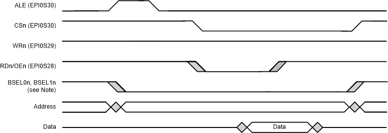
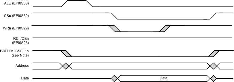
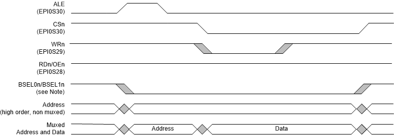
Figure 16-14 shows a write cycle with the address and data signals multiplexed (MODE field is 0x0 in the EPIHBnCFG register). A read cycle would look similar, with the RDn strobe being asserted along with CSn and data being latched on the rising edge of RDn.
When using ALE with dual CSn configuration (CSCFGEXT bit is 0 and the CSCFG field is 0x3 in the EPIHBnCFG2 register) or quad chip select (CSCFGEXT bit is 1 and CSCSFG is 0x2), the appropriate CSn signal is asserted at the same time as ALE, as shown in Figure 16-15.
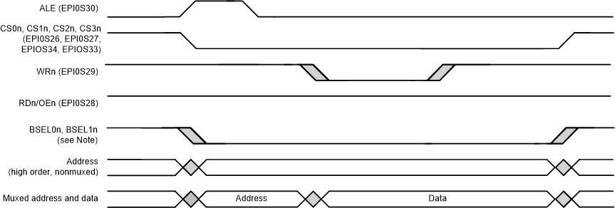
Figure 16-16 shows continuous read mode accesses. In this mode, reads are performed by keeping the read mode selected (output enable is asserted) and then changing the address pins. The data pins are changed by the SRAM after the address pins change.
 Figure 16-16 Continuous Read Mode Accesses
 FIFO mode accesses are the same as normal read and write accesses, except that the ALE signal and address pins are not present. Two input signals can be used to indicate when the XFIFO is full or empty to gate transactions and avoid overruns and underruns. The FFULL and FEMPTY signals are synchronized and must be recognized as asserted by the microcontroller for 2 system clocks before they affect transaction status. The MAXWAIT field in the EPIHBnCFG register defines the maximum number of EPI clock cycles to wait while the FEMPTY or FFULL signal is holding off a transaction. Figure 16-17 shows how the FEMPTY signal should respond to a write and read from the XFIFO. Figure 16-18 shows how the FEMPTY and FFULL signals should respond to 2 writes and 1 read from an external FIFO that contains two entries.
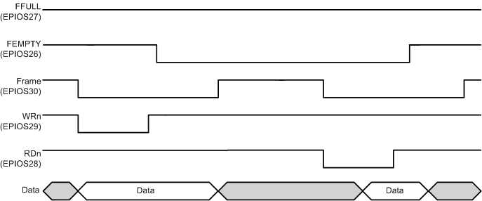 Figure 16-17 Write Followed by Read to External FIFO
  Figure 16-18 Two-Entry FIFO