SLAU748B October 2017 – September 2018 MSP432E401Y
-
SimpleLinkrep%#8482; Ethernet MSP432E401Y Microcontroller LaunchPad™ Development Kit (MSP-EXP432E401Y)
- Trademarks
- 1 Board Overview
- 2 Hardware Description
- 3 Software Development
- 4 PCB Schematics
- Revision History
2.1.6.4 Other Headers and Jumpers
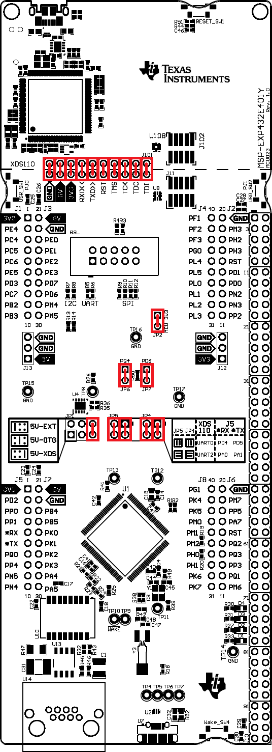
JP1 is provided to select the 5-V power input source for the Ethernet LaunchPad development kit. The left position is for BoosterPack plug-in module power; this position also disconnects both USB voltages from the board’s primary 5-V input. In the left position, the TPS2052B does not limit current so additional care should be exercised. The middle position draws power from the USB connector on the bottom of the board near the Ethernet jack. The right position is the default, in which power is drawn from the XDS-110 USB connection through J101. If JP1 is in the left or middle position, which selects the BoosterPack headers or the USB OTG connector, respectively, externally provide 3.3 V to the board, and remove the 3V3 jumper on J101.
JP2 separates the MCU 3.3-V power domain from the rest of the 3.3-V power on the board allowing an ammeter to be used to obtain more accurate measurements of microcontroller power consumption. JP4 and JP5 are used to configure CAN signals to the BoosterPack Plug-in Module Interface 2 connector. In the default vertical configuration, CAN is not present on the BoosterPack plug-in module connector. UART2 goes to the BoosterPack plug-in module connector and UART 0 goes to the XDS-110 backchannel serial port and can also be used for the ROM serial bootloader. In the horizontal CAN-enabled configuration, UART2 goes to the XDS-110 backchannel serial port and CAN signals are available on the BoosterPack Plug-in Module Interface 2 connector. The ROM serial bootloader is not available to the XDS-110 backchannel serial port while the jumpers are in the CAN position.
Figure 3 shows the default configuration and relative location of the jumpers on the board.
 Figure 3. Default Jumper Locations